Chapter 1 Introduction
Chapter 1 Introduction
Design of Power Management Integrated Circuits 这本教材由德国教授 Bernhard Wicht编写于2020 ~ 2024. 非常好的一本介绍电源芯片系统设计的教材, 贴合工程实践和学术创新.
电源领域近年来蓬勃发展, 手机, 物联网, AI都需要用到越来越高效, 智能的电源产品.
按照下面顺序教学, Chapter1 Introduction - Chapter 7 Linear Voltage Regulators - Chapter 8 Charge Pumps - Chapter 9 Capacitive DC–DC Converters - Chapter 2 Power Stage, Power Transistor- Chapter 3 Semiconductor Devices - Chapter 5 Gate Drivers and Level Shifters - Chapter 6 Protection and Sensing - Chapter 7 Protection and Sensing - Chapter 10 Inductive DC–DC Converters - Chapter 11 Hybrid DC–DC Converters. 因此我们也按照这个顺序review 教材.
1.3 Fundamental Concepts
将12V转化为2V供电可采用下面方法
1.3.1 Using a Resistor – The Linear Regulator
采用LDO, 就是用电阻, 效率低. Chapter 7 介绍
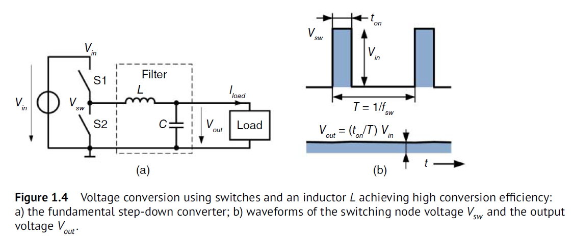
1.3.2 Using Switches and an Inductor – The Inductive DC–DC Converter
采用开关+电感, 效率高可达90%. Chapter 10 介绍
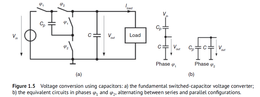
1.3.3 Switches and Capacitors – The SC Converter
采用开关+电容形式, 分1半电压. 12V转6V转3V. 3V转2V可让Cout电容不完全充电, 通过改变frequency可实现
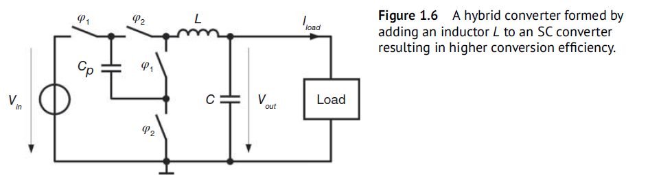
1.3.4 Switches and Capacitors and Inductors – The Hybrid Converter
采用开关+电容+电感形式. 电感可以消除charge redistribution, 降低输出阻抗. 另外LC还能组成resonant tank, 实现软开关. 但注意控制复杂. Chapter 11介绍
1.4 Power Management Systems
手机汽车多电源供电. DCDC, LDO级联. 注意效率为相乘, 𝜂 = 𝜂1 ⋅ 𝜂2
1.5 Applications
1.5.1 IoT Nodes and Energy Harvesting
物联网需要低功耗, 3V 纽扣电池用10年寿命. 需要平均功耗< 2.5uA, 即75.uW. 或者用Energy harvesting 产生1mW供电. Energy harvesting PMIC需要 boost几mV Vin到0.5V - 1V, 然后再换成1.8V
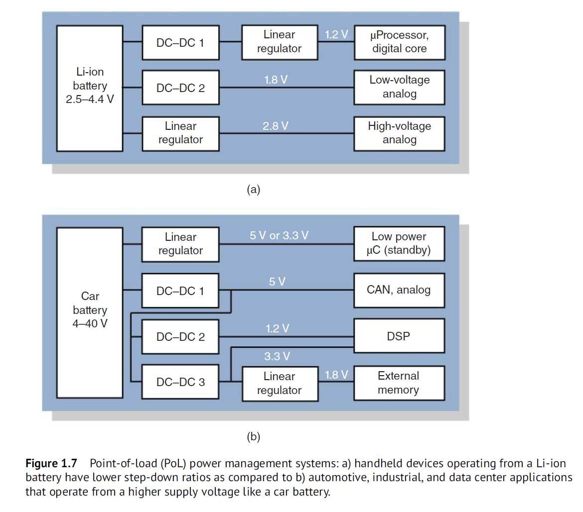
1.5.2 Portable Devices, Smartphones, and Wearables
可穿戴设备, 手机的输入为电池 2.5–4.4V. DC–DC工作在MHz下, 电感得小 uH ~ 几百nH. 要求整体体积小.
1.5.3 Universal Serial Bus (USB)
USB可以传输数据也可以充电. USB power delivery standard (USB-C PD) 可支持100W. 小功率下Vbus=5V, Ibus=3A, 然后Vbus可以继续升到9V, 15V, 最终20V. Ibus也可解锁到5A. 即100W. 不过现在手机私有协议让充电的过程更快, 功率更大.
1.5.4 Drones
无人机功率15-25W, 输入串联电池3-15V-36V.
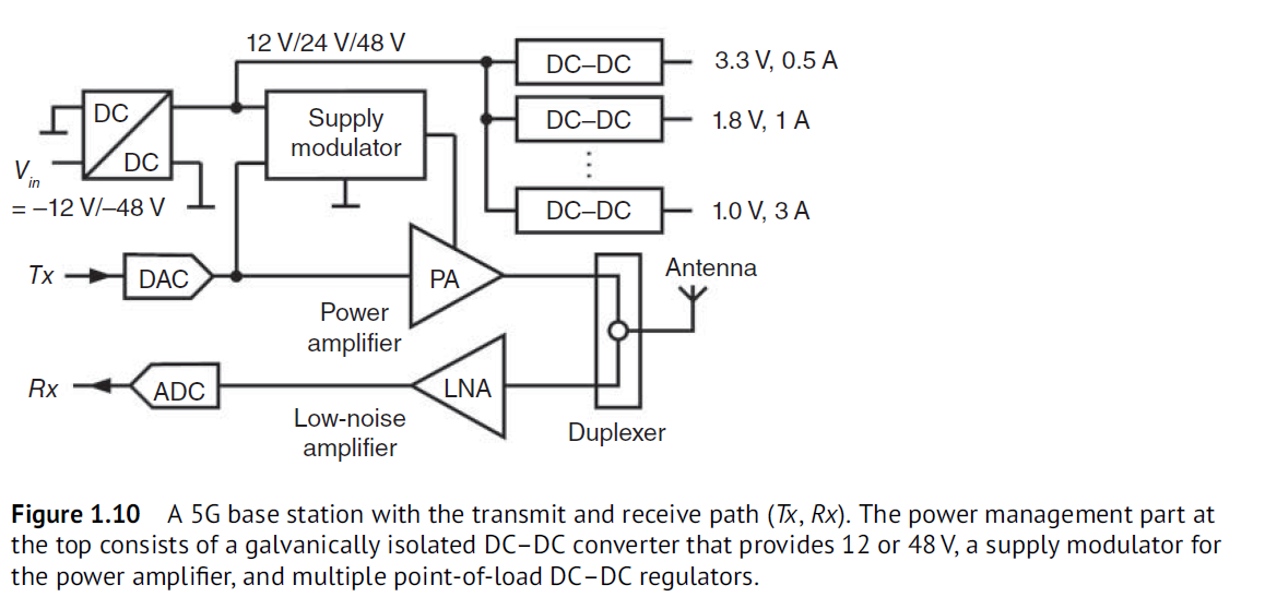
1.5.5 Telecommunication Infrastructure
通信电源, 每个baseband unit (BBU)基带消耗300W, 总共消耗10-20KW.
输入为-24V or -48V, 是为了防止被雷击. 输出为12V/24V/48V. 然后由DC-DC转为3.3V - 1V.
1.5.6 E-Bikes
电瓶车电池为24, 36, or 48V, 功率250W
1.5.7 Automotive
汽车lead-acid battery为12V, 能提供3-5 KW. 电池输入电压能波动到9V- 18V. 考虑冷启动, 输入电压能低到4-6V. 因为电池source resistance 20mΩ, 而starter generator启动需要300A, IR drop达到6V. board net 形成R-L-C网络, board net 电压和负载相关, 这称为load dump. Transient suppressing diodes能钳位board net 电压到36-60V. 因此接到board net线的PMIC输入电压为几V到60V. 温度−40 to 125 ∘C, 甚至节温达到150 ∘C
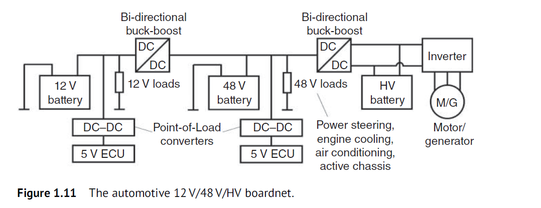
电动车智能化加重了功率. 因此目前趋势是board net从12V提高到48V, 提供8–15 kW. 这样走线电流更小, loss更小. 48V board net变化范围为24-54V.
电车里drive train的Li-ion电池达到400V. Controller Area Network (CAN), 高级辅助驾驶advanced driver assistance systems (ADAS) 目前需要消耗20-30W, 将来耗电会越来越多, 对PMIC是个挑战和机会.
汽车应用还需要注意 electromagnetic interference (EMI), 可用spread-spectrum frequency拓频来解决EMI问题. 汽车电子需要满足 Automotive Safety Integrity Level (ASIL) standards, fail-safe, 需要工作15年.
1.5.8 Data Centers
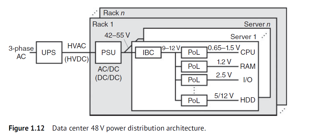
数据中心包括GPU, CPU供电, 是个耗电大户, 功率达到10 MW.
一个Rack功率为10kW - 60kW. 包括 power supply unit (PSU), intermediate bus converter (IBC), point-of-load DC–DC converters (PoL). Rack rail 电压也从12V有趋势增加到48V. 这样能4倍减小输入电流, 即16倍 走线功耗. 但是48V转1V是个挑战.
1.6 IC Supply Voltages
对于先进工艺节点, 供电电压是逐渐降低. 14, 7 nm core supply voltages < 1V. process nodes of 1–2 nm 预计工作在0.65V.
1.7 Power Delivery
考虑PC供电, 12V给CPU供电1V. 目前先进工艺已经不再增加频率, 而是增加晶体管数目来实现更强大功能. CPU需要100A电流. load transient达到5 A/ns. Core电压0.65V, droop电压<10% 要求高.
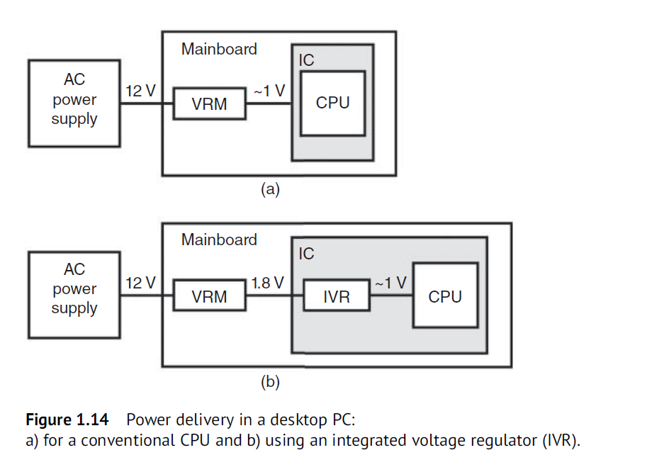
1.7.1 Lateral and Vertical Power Delivery voltage regulator module (VRM)
考虑The routing resistance (mainboard and package) between the VRM and the processor is RPDN = 1.5mΩ. Iload = 100A. 𝜂VRM = 90%.
𝜂tot = Pout/Pin = 100W/ 128W = 78.3%.
1.7.2 Integrated Voltage Regulator (IVR)
内部的 IVR 实现 dynamic voltage and frequency scaling (DVFS) 动态调压. VRM 采用fixed-ratio converter 𝜂VRM = 97%.
IIVR = Vout ⋅ Iload / VIVR ⋅ 𝜂IVR = 1V ⋅ 100 A / 1.8 V ⋅ 0.9 = 61.7 A. 减小了走线损耗.
虽然增加了IVR损耗, 𝜂tot = Pout / Pin = 100W / 120W = 83%.
1.7.3 Dynamic Voltage and Frequency Scaling (DVFS)
数字电路功耗 P = C VDD^2 fclk,
需要N个周期完成task消耗的能量: E = P ⋅ t = NCVDD^2. 因此advanced configuration and power interface (ACPI) 定义 state能 降低电压和频率能大大降低功耗.
1.8 Technology, Components, and Co-integration
1.8.1 Semiconductor Technology
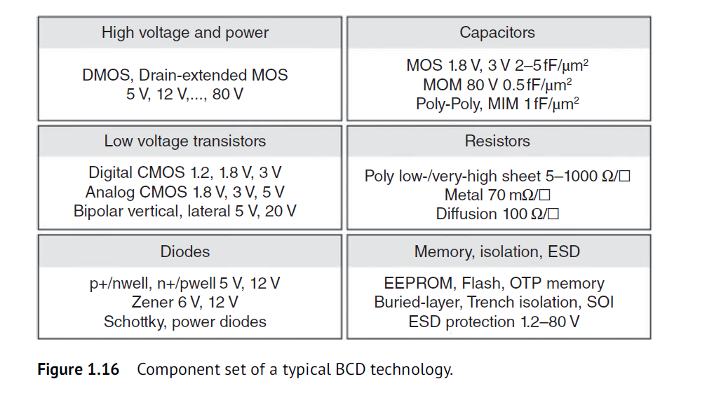
BCD工艺包含BJT和高压CMOS. 需要30+ mask. 省1-2张mask就是省下了6%的钱.
1.8.2 Discrete Power Transistors
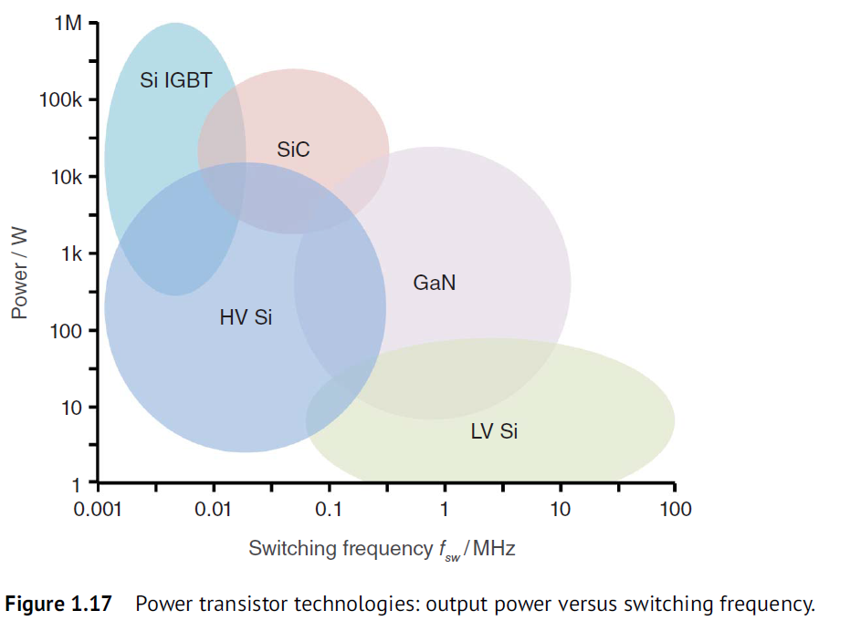
功率器件的耐压, 工作频率范围如下
1.8.3 Passive Components
典型的被动器件由电感电容, L, C ∝ 1∕fsw. 为何DC-DC不做到100MHz呢? Losses, switching loss 和fs成正比 受不了. Speed, 30MHz, ton只有 ~3ns. gate driver很难做. Substrate coupling, noise, 衬底噪声很大, 可通过isolation缓解.
1.8.4 Co-integration
system-in-package (SiP) 电感+电容+芯片合封装
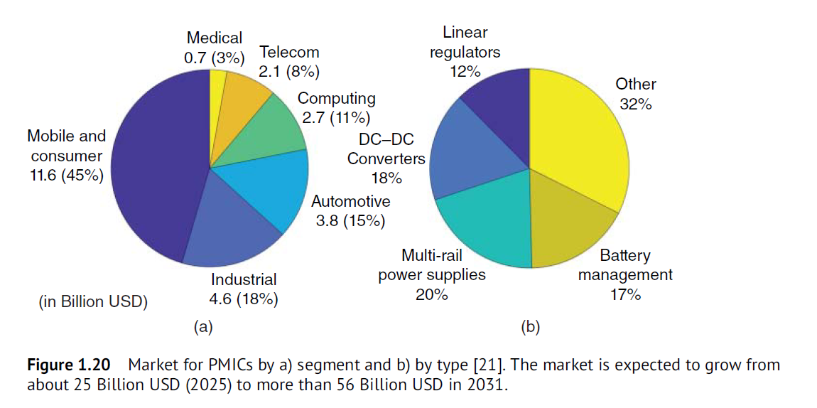
1.9 A Look at the Market
电源占模拟IC的25%, 目前25–30 Billion, 预计2031年到56 billion. 电源大头是手机消费这电子.