技巧小结:外部总线访问FPGA寄存器
概述
需求:stm32的fsmc总线挂载fpga,stm32需要访问fpga内部寄存器
1、分散加载文件将变量存放到指定地址即FPGA寄存器地址
sct文件指定变量存储地址,从而可以直接访问外设,(28335也可以,不过用的是cmd文件),stm32可以将变量指定存放到0x6000 0000地址即外部总线对应的这个地址,而外部总线上这段地址可以是挂载的fpga,也可以是sram等,如果是fpga,fpga会提供寄存器供stm32访问,因此这样访问fpga十分方便;典型代码:
1、修改sct文件新建段FPGA_ADC_REG 0x60000000 UNINIT 0x00000010  {  ; adc data*(.fpga_adc_reg)                       ; 确保段名fpga_adc_reg与代码中一致}
2、源代码定义变量并指定存放地址为段__attribute__((section(".fpga_adc_reg"))) volatile ST_REG ADC_REG[16];
3、直接访问变量就是访问FPGA寄存器ADC_REG[i].all=i;
2、将FPGA寄存器基地址按照指定的结构体形式进行强制类型转换
- 还有一种是定一个一个大的结构体变量
struct fpga,其内部变量的排布格式和fpga提供的一致,然后再将0x6000 0000地址强转为struct fpga类型,对结构体成员的访问也就是对fpga的访问了,这种形式类似于很多stm32底层外设驱动开发格式;典型代码:
1、定义类型
typedef struct
{ST_REG ST_ADC_REG[16];  // adc地址范围0x6000 0000 ~ 0x6000 0010ST_REG ST_PWM_REG[16];  // pwm地址范围0x6000 0010 ~ 0x6000 0020}ST_FPGA_REG; //FPGA所有的寄存器按此结构和顺序排布,如果有空隙则用rsd占位
2、强转类型
#define   fpga_all_regs       (*(volatile ST_FPGA_REG*)0x60000000)
3、访问地址
fpga_all_regs.ST_ADC_REG[i].all=i;
3、指针单独访问FPGA的每个寄存器地址
- 还有一种就是更简单的:地址全部都用宏定义,因为
fpga挂在0x6000 0000地址,每个fpga的变量都是基于此地址偏移,stm32可以直接访问地址,就可以拿到变量值。需要宏定义基地址、偏移地址等等。典型代码:
1、宏定义地址
#define  FPGA_ADDR        (0x60000000)
#define  FPGA_ADC_OFFSET  (0x0)
#define  FPGA_ADC_BASE    (unsigned char*)(FPGA_ADDR+FPGA_ADC_OFFSET)
2、访问地址*(FPGA_ADC_BASE+i) = i;
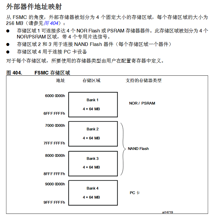
一、FSMC模块
1、FSMC控制寄存器
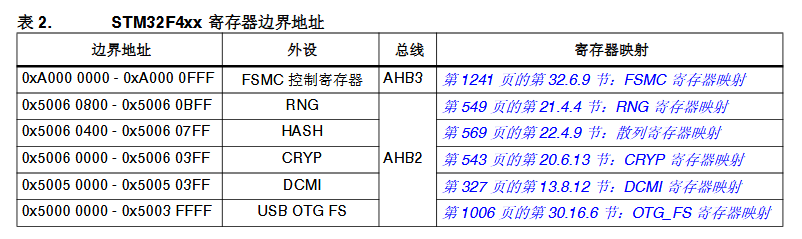
2、FSMC表示的地址范围:
二、访问方式
1、分散加载sct文件指定变量存储地址
sct文件指定变量存储地址,从而可以直接访问外设,(28335也可以,不过用的是cmd文件),stm32可以将变量指定存放到0x6000 0000地址即外部总线对应的这个地址,而外部总线上这段地址可以是挂载的fpga,也可以是sram等,如果是fpga,fpga会提供寄存器供stm32访问,因此这样访问fpga十分方便;
代码例子:
(1)修改分散加载文件生成两个section(段区域)
; *************************************************************
; *** Scatter-Loading Description File generated by uVision ***
; *************************************************************LR_IROM1 0x08000000 0x00100000  {    ; load region size_regionER_IROM1 0x08000000 0x00100000  {  ; load address = execution address*.o (RESET, +First)*(InRoot$$Sections).ANY (+RO).ANY (+XO)}RW_IRAM1 0x20000000 0x00020000  {.ANY (+RW +ZI)}FPGA_ADC_REG 0x60000000 UNINIT 0x00000010  {  ; adc data*(.fpga_adc_reg)                       ; 确保段名fpga_adc_reg与代码中一致}FPGA_PWM_REG 0x60000010 UNINIT 0x00000010  {  ; pwm data*(.fpga_pwm_reg)                       ; 确保段名fpga_pwm_reg与代码中一致}
}
FPGA_ADC_REG这个地方的名字随便起,并不会用到,但是段名fpga_adc_reg是会使用到的!!!UNINIT表示此段无需初始化!!!
(2)定义变量并通过attribute存放到指定地址(执行地址)
typedef struct
{unsigned char bit0:1;unsigned char bit1:1;unsigned char bit2:1;unsigned char bit3:1;unsigned char bit4:1;unsigned char bit5:1;unsigned char bit6:1;unsigned char bit7:1;
}ST_BITS; //位域,按位访问typedef union
{unsigned char all;ST_BITS       bits;
}ST_REG; //按位或者整体访问__attribute__((section(".fpga_adc_reg"))) volatile ST_REG ADC_REG[16];
__attribute__((section(".fpga_pwm_reg"))) volatile ST_REG PWM_REG[16];
ST_REG这种形式既可以按位访问地址,也可以按字节访问地址;volatile表示此变量会被外部设备修改,编译器优化后的代码必须每次都要从内存中访问此变量,而不能从寄存器缓冲中访问;
(3)查看map分配
Load Region LR_IROM1 (Base: 0x08000000, Size: 0x000002f4, Max: 0x00100000, ABSOLUTE)Execution Region ER_IROM1 (Exec base: 0x08000000, Load base: 0x08000000, Size: 0x000002d4, Max: 0x00100000, ABSOLUTE)Exec Addr Load Addr Size Type Attr Idx E Section Name Object0x08000000 0x08000000 0x00000188 Data RO 30 RESET startup_stm32f40xx.o0x08000188 0x08000188 0x00000000 Code RO 36 * .ARM.Collect$$$$00000000 mc_w.l(entry.o)0x08000188 0x08000188 0x00000004 Code RO 39 .ARM.Collect$$$$00000001 mc_w.l(entry2.o)0x0800018c 0x0800018c 0x00000004 Code RO 42 .ARM.Collect$$$$00000004 mc_w.l(entry5.o)0x08000190 0x08000190 0x00000000 Code RO 44 .ARM.Collect$$$$00000008 mc_w.l(entry7b.o)0x08000190 0x08000190 0x00000000 Code RO 46 .ARM.Collect$$$$0000000A mc_w.l(entry8b.o)0x08000190 0x08000190 0x00000008 Code RO 47 .ARM.Collect$$$$0000000B mc_w.l(entry9a.o)0x08000198 0x08000198 0x00000004 Code RO 54 .ARM.Collect$$$$0000000E mc_w.l(entry12b.o)0x0800019c 0x0800019c 0x00000000 Code RO 49 .ARM.Collect$$$$0000000F mc_w.l(entry10a.o)0x0800019c 0x0800019c 0x00000000 Code RO 51 .ARM.Collect$$$$00000011 mc_w.l(entry11a.o)0x0800019c 0x0800019c 0x00000004 Code RO 40 .ARM.Collect$$$$00002712 mc_w.l(entry2.o)0x080001a0 0x080001a0 0x00000024 Code RO 31 .text startup_stm32f40xx.o0x080001c4 0x080001c4 0x00000024 Code RO 55 .text mc_w.l(init.o)0x080001e8 0x080001e8 0x00000002 Code RO 1 i.SystemInit main.o0x080001ea 0x080001ea 0x0000000e Code RO 59 i.__scatterload_copy mc_w.l(handlers.o)0x080001f8 0x080001f8 0x00000002 Code RO 60 i.__scatterload_null mc_w.l(handlers.o)0x080001fa 0x080001fa 0x0000000e Code RO 61 i.__scatterload_zeroinit mc_w.l(handlers.o)0x08000208 0x08000208 0x0000009c Code RO 2 i.main main.o0x080002a4 0x080002a4 0x00000030 Data RO 57 Region$$Table anon$$obj.oExecution Region RW_IRAM1 (Exec base: 0x20000000, Load base: 0x080002d4, Size: 0x00000400, Max: 0x00020000, ABSOLUTE)Exec Addr Load Addr Size Type Attr Idx E Section Name Object0x20000000 - 0x00000400 Zero RW 28 STACK startup_stm32f40xx.oExecution Region FPGA_ADC_REG (Exec base: 0x60000000, Load base: 0x080002d4, Size: 0x00000010, Max: 0x00000010, ABSOLUTE, UNINIT)Exec Addr Load Addr Size Type Attr Idx E Section Name Object0x60000000 0x080002d4 0x00000010 Data RW 3 .fpga_adc_reg main.oExecution Region FPGA_PWM_REG (Exec base: 0x60000010, Load base: 0x080002e4, Size: 0x00000010, Max: 0x00000010, ABSOLUTE, UNINIT)Exec Addr Load Addr Size Type Attr Idx E Section Name Object0x60000010 0x080002e4 0x00000010 Data RW 4 .fpga_pwm_reg main.o
0x20000000是默认的RAM区域,也是片上RAM对应的地址,用给其他所有的RW和ZI变量,这里的0x20000000是执行地址,即程序运行后要访问变量时是访问执行地址;
0x60000000是FSMC模块对应给FPGA寄存器变量的地址,这里的0x60000000是执行地址,即程序运行后要访问FPGA寄存器时是访问执行地址0x60000000;加载地址是0x080002d4,也就是为RW属性,变量需要从ROM的0x080002d4取出数据加载到执行地址0x60000000里作为初值!而.fpga_adc_reg 是这个区域内部的一个段,也就是用户程序会用到的段。
(4)访问变量
  for(unsigned char i = 0; i<16;i++){ADC_REG[i].all=i;PWM_REG[i].bits.bit0 = i+0;}
ADC_REG[0]的地址就是0x60000000
ADC_REG[1]的地址就是0x60000001
ADC_REG[2]的地址就是0x60000002
...
ADC_REG[15]的地址就是0x6000000FPWM_REG[0]的地址就是0x60000010
...
PWM_REG[15]的地址就是0x6000001F
2.地址强转为自定义的结构体类型
还有一种是定一个一个大的结构体变量struct fpga,其内部变量的排布格式和fpga提供的一致,然后再将0x6000 0000 地址强转为struct fpga类型,对结构体成员的访问也就是对fpga的访问了,这种形式类似于很多stm32底层外设驱动开发格式;
代码例子:
(1)定义FPGA寄存器的格式
typedef struct
{unsigned char bit0:1;unsigned char bit1:1;unsigned char bit2:1;unsigned char bit3:1;unsigned char bit4:1;unsigned char bit5:1;unsigned char bit6:1;unsigned char bit7:1;
}ST_BITS; //位域,按位访问typedef union
{unsigned char all;ST_BITS       bits;
}ST_REG; //按位或者整体访问typedef struct
{ST_REG ST_ADC_REG[16];  // adc地址范围0x6000 0000 ~ 0x6000 0010ST_REG ST_PWM_REG[16];  // pwm地址范围0x6000 0010 ~ 0x6000 0020}ST_FPGA_REG; //FPGA所有的寄存器按此结构和顺序排布,如果有空隙则用rsd占位
fpga提供两组寄存器,分别是ADC和PWM模块的,两者的寄存器紧挨着放置,顺序就是ST_FPGA_REG声明的那样。
(2)定义FPGA寄存器的地址
#define FPGA_ADDR (0x60000000)
(3)强制转换FPGA寄存器的地址为ST_FPGA_REG类型
#define fpga_all_regs (*(volatile ST_FPGA_REG*)FPGA_ADDR)这里需要进一步理解指针:指针提供两个信息:从哪个地址开始按照什么格式区看后面的数据。比如,(ST_FPGA_REG*)0x60000000表示从0x60000000地址访问数据,这个地址后面的数据要按照ST_FPGA_REG格式去阅读和访问(即指针指向的类型);带上*号表示对此地址解引用即访问此地址,需要按照ST_FPGA_REG格式去访问。
(4)访问FPGA的寄存器值
for(unsigned char i = 0; i<16;i++){ fpga_all_regs.ST_ADC_REG[i].all=i;fpga_all_regs.ST_PWM_REG[i].bits.bit0 = i+0;}
3.指针访问宏定义的地址
还有一种就是更简单的:地址全部都用宏定义,因为fpga挂在0x6000 0000地址,每个fpga的变量都是基于此地址偏移,stm32可以直接访问地址,就可以拿到变量值。需要宏定义基地址、偏移地址等等。
代码例子:
(1)定义FPGA寄存器地址
#define   FPGA_ADDR       (0x60000000)#define  FPGA_ADC_OFFSET  (0x0)
#define  FPGA_PWM_OFFSET  (0x10)//需要指定地址的类型即指向哪种数据类型,默认设置为unsigned char
#define  FPGA_ADC_BASE    (unsigned char*)(FPGA_ADDR+FPGA_ADC_OFFSET)
#define  FPGA_PWM_BASE    (unsigned char*)(FPGA_ADDR+FPGA_PWM_OFFSET)#define  FPGA_ADC_SIZE    (0x10)
#define  FPGA_PWM_SIZE    (0x10)
宏定义定义地址时需要指定地址的指向类型,可以默认为unsigned char。
(2)访问FPGA寄存器
for(unsigned char i = 0; i<FPGA_ADC_SIZE; i++){ *(FPGA_ADC_BASE+i) = i;*(FPGA_PWM_BASE+i) = i+1; //此时无法使用结构体按位访问了(*(ST_REG*)(FPGA_ADC_BASE+i)).all = i;(*(ST_REG*)(FPGA_PWM_BASE+i)).bits.bit0 = i+1; //强转之后就能用结构体按位访问了}
对地址直接解引用访问则为unsigned char类型,无法按位访问。可以先强制转换为ST_REG类型,就可以对字节进行按位访问了。
三、所有代码
所有代码
1、sct文件
; *************************************************************
; *** Scatter-Loading Description File generated by uVision ***
; *************************************************************LR_IROM1 0x08000000 0x00100000  {    ; load region size_regionER_IROM1 0x08000000 0x00100000  {  ; load address = execution address*.o (RESET, +First)*(InRoot$$Sections).ANY (+RO).ANY (+XO)}RW_IRAM1 0x20000000 0x00020000  {.ANY (+RW +ZI)}FPGA_ADC_REG 0x60000000 UNINIT 0x00000010  {  ; adc data*(.fpga_adc_reg)                       ; 确保段名fpga_adc_reg与代码中一致}FPGA_PWM_REG 0x60000010 UNINIT 0x00000010  {  ; pwm data*(.fpga_pwm_reg)                       ; 确保段名fpga_pwm_reg与代码中一致}
}
2、map表
==============================================================================Memory Map of the imageImage Entry point : 0x08000189Load Region LR_IROM1 (Base: 0x08000000, Size: 0x000002d4, Max: 0x00100000, ABSOLUTE)Execution Region ER_IROM1 (Exec base: 0x08000000, Load base: 0x08000000, Size: 0x000002b4, Max: 0x00100000, ABSOLUTE)Exec Addr Load Addr Size Type Attr Idx E Section Name Object0x08000000 0x08000000 0x00000188 Data RO 30 RESET startup_stm32f40xx.o0x08000188 0x08000188 0x00000000 Code RO 36 * .ARM.Collect$$$$00000000 mc_w.l(entry.o)0x08000188 0x08000188 0x00000004 Code RO 39 .ARM.Collect$$$$00000001 mc_w.l(entry2.o)0x0800018c 0x0800018c 0x00000004 Code RO 42 .ARM.Collect$$$$00000004 mc_w.l(entry5.o)0x08000190 0x08000190 0x00000000 Code RO 44 .ARM.Collect$$$$00000008 mc_w.l(entry7b.o)0x08000190 0x08000190 0x00000000 Code RO 46 .ARM.Collect$$$$0000000A mc_w.l(entry8b.o)0x08000190 0x08000190 0x00000008 Code RO 47 .ARM.Collect$$$$0000000B mc_w.l(entry9a.o)0x08000198 0x08000198 0x00000004 Code RO 54 .ARM.Collect$$$$0000000E mc_w.l(entry12b.o)0x0800019c 0x0800019c 0x00000000 Code RO 49 .ARM.Collect$$$$0000000F mc_w.l(entry10a.o)0x0800019c 0x0800019c 0x00000000 Code RO 51 .ARM.Collect$$$$00000011 mc_w.l(entry11a.o)0x0800019c 0x0800019c 0x00000004 Code RO 40 .ARM.Collect$$$$00002712 mc_w.l(entry2.o)0x080001a0 0x080001a0 0x00000024 Code RO 31 .text startup_stm32f40xx.o0x080001c4 0x080001c4 0x00000024 Code RO 55 .text mc_w.l(init.o)0x080001e8 0x080001e8 0x00000002 Code RO 1 i.SystemInit main.o0x080001ea 0x080001ea 0x0000000e Code RO 59 i.__scatterload_copy mc_w.l(handlers.o)0x080001f8 0x080001f8 0x00000002 Code RO 60 i.__scatterload_null mc_w.l(handlers.o)0x080001fa 0x080001fa 0x0000000e Code RO 61 i.__scatterload_zeroinit mc_w.l(handlers.o)0x08000208 0x08000208 0x0000007c Code RO 2 i.main main.o0x08000284 0x08000284 0x00000030 Data RO 57 Region$$Table anon$$obj.oExecution Region RW_IRAM1 (Exec base: 0x20000000, Load base: 0x080002b4, Size: 0x00000400, Max: 0x00020000, ABSOLUTE)Exec Addr Load Addr Size Type Attr Idx E Section Name Object0x20000000 - 0x00000400 Zero RW 28 STACK startup_stm32f40xx.oExecution Region FPGA_ADC_REG (Exec base: 0x60000000, Load base: 0x080002b4, Size: 0x00000010, Max: 0x00000010, ABSOLUTE, UNINIT)Exec Addr Load Addr Size Type Attr Idx E Section Name Object0x60000000 0x080002b4 0x00000010 Data RW 3 .fpga_adc_reg main.oExecution Region FPGA_PWM_REG (Exec base: 0x60000010, Load base: 0x080002c4, Size: 0x00000010, Max: 0x00000010, ABSOLUTE, UNINIT)Exec Addr Load Addr Size Type Attr Idx E Section Name Object0x60000010 0x080002c4 0x00000010 Data RW 4 .fpga_pwm_reg main.o==============================================================================
3、源代码
/*   1、分散加载文件指定变量存放地址    */
typedef struct
{unsigned char bit0:1;unsigned char bit1:1;unsigned char bit2:1;unsigned char bit3:1;unsigned char bit4:1;unsigned char bit5:1;unsigned char bit6:1;unsigned char bit7:1;
}ST_BITS; //位域,按位访问typedef union
{unsigned char all;ST_BITS       bits;
}ST_REG; //按位或者整体访问__attribute__((section(".fpga_adc_reg"))) volatile ST_REG ADC_REG[16];
__attribute__((section(".fpga_pwm_reg"))) volatile ST_REG PWM_REG[16];  /*   2、强制转换地址为结构体格式       */
typedef struct
{ST_REG ST_ADC_REG[16];  // adc地址范围0x6000 0000 ~ 0x6000 0010ST_REG ST_PWM_REG[16];  // pwm地址范围0x6000 0010 ~ 0x6000 0020}ST_FPGA_REG; //FPGA所有的寄存器按此结构和顺序排布,如果有空隙则用rsd占位#define   FPGA_ADDR   (0x60000000)
#define   fpga_all_regs       ( *(volatile ST_FPGA_REG*)FPGA_ADDR)/*             3、指针访问           */
#define  FPGA_ADC_OFFSET    (0x0)
#define  FPGA_PWM_OFFSET    (0x10)//需要指定地址的类型即指向哪种数据类型,默认设置为unsigned char
#define  FPGA_ADC_BASE    (unsigned char*)(FPGA_ADDR+FPGA_ADC_OFFSET)
#define  FPGA_PWM_BASE    (unsigned char*)(FPGA_ADDR+FPGA_PWM_OFFSET)#define  FPGA_ADC_SIZE    (0x10)
#define  FPGA_PWM_SIZE    (0x10)/***   主函数*/
int main(void)
{	unsigned char i= 0;/*   1、分散加载文件指定变量存放地址    */for(i = 0; i<16;i++){ADC_REG[i].all=i;PWM_REG[i].bits.bit0 = i+0;}/*   2、强制转换地址为结构体格式       */for(i = 0; i<16;i++){	fpga_all_regs.ST_ADC_REG[i].all=i;fpga_all_regs.ST_PWM_REG[i].bits.bit0 = i+0;}/*             3、指针访问           */for(i = 0; i<FPGA_ADC_SIZE; i++){	*(FPGA_ADC_BASE+i) = i;*(FPGA_PWM_BASE+i) = i+1; //此时无法使用结构体按位访问了(*(ST_REG*)(FPGA_ADC_BASE+i)).all = i;(*(ST_REG*)(FPGA_PWM_BASE+i)).bits.bit0 = i+1; //强转之后就能用结构体按位访问了}while(1){}}