Chapter 9 Capacitive DC–DC Converters
Chapter 9 Capacitive DC–DC Converters
Capacitive DC–DC converters 通过电容和管子实现DC-DC, 也称为switched-capacitor converters or SC converters. 由于电容高储能性, 而且不像LDO一样效率低下, 因此很受欢迎. 这种converter 适用于 fully integrated point-of-load power supplies (power-supply-on-chip). 对于更大电流, 可采用片外电容, 也是一个compact solution.
9.1 Introduction
下图展示了基本2:1 SC converter. C1在SC converter中被称为flying capacitor. 任何降压SC converter, 输入输出反过来也是升压converter.

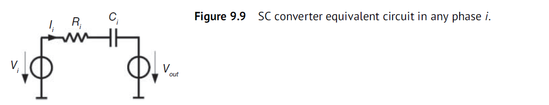
任何SC converter可以用下面电路建模: 理想变压器+串联+并联电阻.

理想变压器为1: Ni 为iLoad=0A转换比.

Rout输出阻抗决定 Vout drop电压, Rout取决于开关频率, Cfly电容值和switch阻抗.
Rp并联变压器副端, 为extrinsic loss, 代表gate driver losses
因此输出Vout表达式为
V
o
u
t
=
N
i
V
i
n
−
R
o
u
t
I
l
o
a
d
V_{out} = N_iV_{in} − R_{out}I_{load}
Vout=NiVin−RoutIload
真实的转换比

SC converter效率为

类似LDO, SC converter效率由输出电压/输入电压. 我们设计的目标就是尽量减小Rout
9.2 Realizable Ratios
1995年groundbreaking work by Makowski and Maksimovic´ 证明 n个flying cap能产生的ideal conversion ratios Ni 为

1个cfly能产生1:2. 两个cfly能产生1: 3,1:2和2/3. 如下图所示, Fig 7.3(a) 所有电容串联+并联 形成3:1结构. (b) 两电容串联+并联形成3:2结构.

9.3 Switched-Capacitor Topologies
这小节介绍常见的SC架构: series–parallel, the Dickson, the ladder, and the Fibonacci topology 如下图所示, 以3:1架构为例
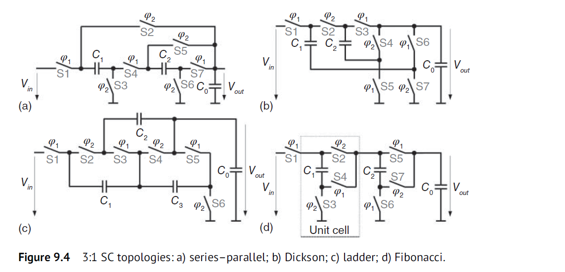
9.3.1 Series–Parallel
串并联结构如Fig 9.3(a)所示, 用7个switch和2个Cfly, 我们关心管子和电容看到最大电压, 耐压越小, 相同阻抗面积越小. Fig 9.4(a)中 S1 and S2 see a maximum voltage of 2Vout (S1 during 𝜑2 and S2 during 𝜑1). 优点是Cfly看到的电压只有Vout. 另外在switch 𝜑1左侧添加一个电容+switch, 再加上一个接到Vout的𝜑2 switch就能形成4:1 串并联结构.
9.3.2 Dickson
Dickson架构如Fig 9.3(b), 类似Fig 8.10, 用上拉和下拉switch替代了Fig 8.10中的inverter. C1看到2Vout, C2看到Vout, S2需要承受2Vout. 其他开关承受Vout. 在S1和Vin之间再加一个switch和电容能进一步降低转换比. C1和S2永远是承压最大的.


9.3.3 Ladder
Ladder有两row电容, C1+C3和C2. 电容row在Vin,Vout和gnd之间切换. Ladder结构的优点是所有电容和开关的耐压都是Vout, 缺点是比起其他结构, Ladder所需电容多一个. 由于每个电容电压都是Vout, 因此ladder结构可做floating gate supply, 这是ladder独有的优势.

9.3.4 Fibonacci
Fibonacci结构能形成1,3,5,8的转换比. C1和S2耐压2Vout. S4耐压2Vout

9.3.5 Conclusion
转换比Ni = 2, 所有架构都是一样.
只有一些架构能实现9.2小节理论上的转换比
在启动时, 一些电容和开关能看到Vin, 因此需要clamping和pre-charging电路, 来防止器件烧毁或者过压. shunt-regulators, LDO, high-resistive (power dissipation!) voltage dividers和diode-connected管子需要用来pre-charge. 等conveter建立好后, pre-charge电路再disable.
9.4 Gate Drive Techniques
SC converter的驱动功率干开关需要特别注意. 对于开关一端接地, 可以直接驱动. 对于高边开关, 如果switching node能为gnd, 可用bootstrap. 对于switching nodes不回到gnd, 可用charge pump结构, Section 8.9介绍. 如下图的M3和M4. 一些SC converter需要Vout, 2Vout, 3Vout电源轨, 可用ladder SC做gate驱动电源.

9.5 Charge Flow Analysis
我们可以通过charge flow电荷流动的方法计算通过电容和开关的电流, Seeman and Sanders在其thesis中介绍过.
9.5.1 Charge Flow Vectors
Capacitor Charge Flow Vectors
各电容charge为 q1, q2, qn. 输出电容charge为qout=Iload*Ts.
每个电容电荷守恒, 即和为零.

ai代表各电容charge/输出电容charge的值, 即归一化

Switch Charge Flow Vectors
开关switch流过的charge/qout也可以归一化系数. ar表示为

9.5.2 Charge Flow Vectors of Common Topologies
对于SC converter, 我们先画出, 列出在每个phase所有电容和开关流过的charge. 利用电容电荷守恒, 列出等式. 需要注意charge流过方向, 有正有负.
Ladder converter的qx最难定义
Fig 9.7 列举了a) series–parallel; b) Dickson; c) ladder; d) Fibonacci 4种架构 charge flow的示意图

charge flow总结为Table 9.3

9.5.3 Ideal Conversion Ratio
计算conversion ratio, 统计输入电流Iin = qin*fsw. 输入功率=输出功率
Pin = Vin* Iin = Vin *qin *fsw
Pout = VoutI* load = Vout qout fsw
Pin=Pout, 因此Vin qin fsw = Vout qout fsw
ideal conversion ratio
N
i
=
V
o
u
t
V
i
n
=
q
i
n
q
o
u
t
=
a
i
n
a
o
u
t
N_{i}=\frac{V_{out}}{V_{in}}=\frac{q_{in}}{q_{out}}=\frac{a_{in}}{a_{out}}
Ni=VinVout=qoutqin=aoutain
对于2:1 converter
N
i
=
V
o
u
t
V
i
n
=
a
i
n
a
o
u
t
=
1
/
2
+
0
1
/
2
+
1
/
2
=
1
2
N_{i}=\frac{V_{out}}{V_{in}}=\frac{a_{in}}{a_{out}}=\frac{1/2+0}{1/2+1/2}=\frac{1}{2}
Ni=VinVout=aoutain=1/2+1/21/2+0=21
也可得3:1 topology得Ni=1/3
9.5.4 Equivalent Output Resistance
SC converter得输出阻抗Rout表示Cfly和Switch产生的loss.

Rout由slow and fast-switching limits (SSL, FSL)渐近线表示

Slow-Switching Limit (SSL)
SSL表示switch没有电阻, Loss即Rout全部由Cfly决定.
我们知道对一个电容充电ΔV, 会产生1/2 C ΔV^2的loss

我们统计所有充放电Cfly电容上能量损失

转化为RSSL为电荷比, 认为输出电容没有loss.

对于基本的2:1结构
R
S
S
L
=
1
4
C
j
f
s
w
R_{SSL}=\frac{1}{4C_jf_{sw}}
RSSL=4Cjfsw1
假设C1=C2=C, 对于3:1 series–parallel架构, RSSL为

3:1 的Dickson 和Fibonacci RSSL为

KSSL定义为把ac,j和各phase加到一起.

Fast-Switching Limit (FSL)
当频率fs越来越高时, 输出阻抗即loss由fast switching limit决定, 即开关switch 的Ron. Rout=RFSL,

对于2:1 的SC Converter, RFSL为
R
F
S
L
=
2
R
R_{FSL}=2R
RFSL=2R
对于3:1的ladder, RFSL为

对于3:1的series–parallel and Dickson, RFSL为

相似的, K定义为各phase, ar加到一起

Total Output Resistance
输出阻抗Rout近似为RSSL和RFSL的平方根, 拟合的很好了!
R
o
u
t
=
R
S
S
L
2
+
R
F
S
L
2
R_{out}=\sqrt{R_{SSL}^{2}+R_{FSL}^{2}}
Rout=RSSL2+RFSL2
Full Derivation of Rout
关于Rout的完整推导, 可把switch和C串联视为RC串联, 求得流过switch和电容的电流i的表达式
然后推导出Rout为

9.6 Output Voltage Ripple
SC Converter输出电压纹波为

kd 为 discharge fraction factor, Co*为有效输出电容.
kd expresses how often per switching period charge is delivered to the output by the flying capacitor(s). 对于2:1 SC converter, kd=2, 因为在一个周期内, Cfly两次给Cout充电.
Co*的有效电容取决于Cout和Cfly.
9.7 Topology Selection
对于SC converter拓扑选择, 需要考虑一下几个因素
● Realizable conversion ratio(s) (see Sections 9.2 and 9.5.2) 可实现的转换比
● Number of flying capacitors n 所需Cfly个数n
● Maximum capacitor voltage Vmax,c 电容最大耐压
● Number of switches nsw 开关个数nsw
● Maximum blocking voltage of the switches Vmax,sw 开关耐压! 这个很重要
● Ideal conversion ratio(s) (see Section 9.5.3) 理想转换比
● Achievable equivalent output resistance (see Section 9.5.4) Rout值影响loss和输出
● Gate drive effort 驱动复杂度
● Control effort 控制复杂度
Series–Parallel, Dickson, Ladder, and Fibonacci的关键参数总结如下:

9.8 Capacitor and Switch Sizing
电容越大, 输出纹波越小.
9.8.1 Flying Capacitor Sizing
以Ctot作为预算约束, 每个Cfly电容值为

可得RSSL为

Eg, Ctot = 8nF, 工作在fsw = 10MHz.
对于3:1 dickson, since the charge flow in both flying capacitors of the Dickson topology is equal, the capacitors are identical in size, and we obtain C1 = C2 = 4nF. dickson C1和C2的charge flow相同.

可得Ladder和Dickson的Rout为下图. Dickson的RSSL是Ladder的1/4.

9.8.2 Switch Sizing
以Wtot 为所有管子的 widths 之和作为预算约束 因此每个管子的W/L size为

RFSL为

Examples 9.4, Wtot= 8mm, Vth = 0.6V, VGS = 5V, and 𝜇oCox = 75 μA/V2.
对于Dickson, 所有switch charge flow一样. 可得每个switch size为8/7mm
因此每个管子的Ron和RFSL可得

或者用Gtot计算, 可得相同结果.

对于Ladder, Switches S1–S4的size为8mm/8=1mm. S5 and S6 的W = 2.0mm. 可得RFSL为

9.8.3 Output Capacitor Sizing
以Vout peak-peak为target, Ctot为限制, 可得Co为

Examples 9.5 需要设计ΔVout,pkpk = 50mV, fsw = 10MHz and Iload = 5 mA.
Dickson and Ladder have the flying capacitors connected to Vout in each phase, we always have kd = 2
C1 = C2 = 4nF and Ctot = 8nF, kt, is already derived in Example 9.3 for both 3:1

For lower ripple, Co has to be increased to much higher values than C1 and C2. 对于低ripple设计, 需要设计Co >> C1,C2.
9.9 Loss Analysis and Efficiency
9.9.1 Intrinsic Losses
Rout引入的Loss为intrinsic loss
P
r
o
u
t
=
I
l
o
a
d
2
R
o
u
t
P_{rout}=I^{2}_{load}R_{out}
Prout=Iload2Rout
以Examples 9.4, 9.5 的3:1 Dickson为例.Iload = 100 mA
RSSL = 5.6Ω and RFSL = 1.24Ω, 因此可得Rout和intrinsic losses

9.9.2 Switch Control Losses
gate charge loss为. Vdrv为功率管Vgs.

Example 9.9
3:1 Dickson topology at fsw = 10MHz. L = Lmin = 0.3 μm, Vth = 0.6V, VGS = 5V, 𝜇o = 500 ×10−4 m2/(Vs), Cox = 1.5 × 10⁻³ F/m2.
Eg 9.5算得W = 1.14mm. 因此可得Cgate, Pgate_单管和Pgate_total

可以看到gate loss还是较低的, 可以通过增加size 降低Rout
9.9.3 Parasitic Capacitor Bottom-Plate Losses
以2:1 SC为例, 如下图所示
top-plate 寄生电容 Ctp 可传输charge到Vout, loss几乎忽略不计
bottom-plate 寄生电容Cbp在Phase 2, 就接到Gnd, charge白白损失了. 因此Cbp为主要loss来源.

Cbp = 𝛾C1. 𝛾 取决于电容类型, ∼10% for MOS capacitors down to a few percent for MIM capacitors. 因此Pbp引入的loss为

Example 9.10 fsw = 50MHz, Ctot = 8nF, 𝛾 = 0.03 (3%). Vout = 1.8V. 算得Pbp为

Section 4.1小节介绍如何减少Cbp. 另外由于Cbp > Ctp, 可以让C1颠倒. Also, high-resistively biased wells can be placed underneath the flying capacitor C1. Charge recycling techniques of the parasitic bottom-plate capacitance during the dead time between the phases 𝜑1 and 𝜑2 can be applied [13, 14]. It can be very effective if the input voltages and switching frequencies are low.
9.9.4 Static Losses
内部电源Vdd需要Idd得bias current. Vdd来源于Vin, 可由LDO或者shunt regulator产生, 因此效率有损失

9.9.5 Loss Minimization

为了最小化Loss
- SC 整体loss需要在RSSL和RFSL之间平衡. 更大size的switch降低RFSL, 但是Cap值更小, RSSL会增大.
- 在低频时注意PRout 和 Pbp trade-off
- 在高频时注意Pgate会增加.
作为初始设计点, 可设计fs频率, 让RSSL=RFSL

9.9.6 Total Losses
整体功耗为所有Loss加到一起.

9.9.7 Efficiency

9.10 Multi-phase SC Converters
为了得到其他conversion ratio, 可添加 phase, 即增加switch或者添加开关on/off组合.
对于3:1 Fibonacci topology, 没有添加Cfly和Switch, 仅通过增加开关组合, 实现了4:1的转换比. 如下图所示

3个电容Charge Flow为

4个管子charge flow为

另外需要注意某些管子可能需要正向/反向都要档电压, 因此管子需要back-to-back 结构
9.11 Multi-ratio SC Converters
多转换比的SC可通过改变开关phase来实现. 每到1/N的转换比那个点, 效率才能上升, 在1/2 ~ 1/3 中间效率较差.

9.11.1 Multi-ratio Implementation of Common SC Topologies
下图结构可实现1/3, 1/2, 2/3d的转换比. 需要1/2时S4 off. 形成two separate 2:1 series–parallel stages that operate in parallel

9.11.2 Folding Dickson
对于5:1的dickson, 通过电容合并, 可实现5:1, 4:1, 3:1和2:1转换比, 如下图所示

9.11.3 SAR SC Converters
successive approximation register SC converters (SAR SC converters) 逐次逼近SAR SC很有意思. 采用N位 2:1的SC, 输出resolution为

N位bit, 每个bit输入可接high ,即Vin和Vout之间, (Vhigh + Vlow)∕2. 或者接low 即Vout和gnd之间.
对于binary configuration code B, 可算出输出电压为

Vin=2V, Vout=1.25V, B=1001.

9.11.4 Recursive SC Converters
Recursive SC (RSC) 在sar SC 基础上更进一步, 它充分利用了所有Cfly电容. 如下图所示

9.12 Multi-phase Interleaving
为了减小SC输出电压ripple, 可采用多相SC, 如下图所示. 每路phase shift为180∘ / nst

因此输出Vout ripple为

Kd是discharge fraction factor. For the basic 2:1 SC stage, kd = 2.
输出电容Co能减小4倍, 很省面积!
9.13 Control Methods
为了得到精准的DC输出电压和快速响应, SC需要控制环路, 来控制Rout, 从而控制Vout.
V
o
u
t
=
N
i
V
i
n
−
R
o
u
t
I
l
o
a
d
V_{out}=N_{i}V_{in}-R_{out}I_{load}
Vout=NiVin−RoutIload
Rout由RSSL和RFSL组成, RSSL和频率, Ctot成反比. RFSL和duty cycle D成反比, 和Rdson成正比.

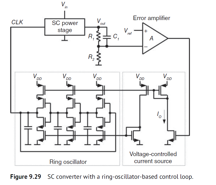
pulse-frequency modulation (PFM) 是 SC中最常见的频率控制手段.
考虑下图结构, The current-starved ring oscillator 形成 VCO. EA决定SC的输出. Vout通过resistor divider和Vref相比较. 当Vout下降, EA输出增加, Io增加, 因此ring OSC频率增加, 导致SC输出增加.
C1 in parallel to R1 in the resistive divider implements lead compensation of the control loop [11]. A stable control loop is obtained by positioning the zero at the error amplifier’s 3 dB frequency and by shifting all higher-order poles beyond the switching frequency
另外还可以通过改变Cfly, 通过电容矩阵. 或者通过电阻开关矩阵, 或者通过改变duty cycle D 来改变输出电压.