PCIe - ZCU106(RC) + KU5P(EP) + 固化
目录
1. 简介
1.1 Data Mover
1.2 描述符
2. ZCU102
2.1 Ubuntu OS
2.2 USB Host
2.2.1 连接拓扑
2.2.2 设备类型
2.2.3 USB 跳帽设置
2.3 无线网卡
2.4 PCIe Info
2.4.1 Diagram
2.4.2 lspci -tv
2.4.3 lspci -v
2.4.2.1 设备基本信息
2.4.2.2 控制与状态寄存器
2.4.2.3 中断与总线拓扑
2.4.2.4 地址空间配置
2.4.2.5 桥接器控制与能力
2.4.2.6 内核驱动
2.4.4 setpci
2.4.5 命令汇总
3. ZCU102+KU5P
3.1 vivado 工程
3.1.1 Block Design
3.1.2 IBUFDS_GTE
3.1.3 XDMA PCIe
3.1.4 Address Editor
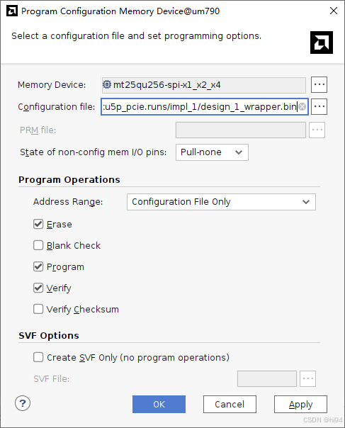
3.1.5 烧写与固化
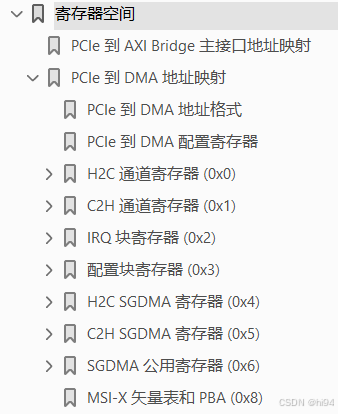
3.2 寄存器空间
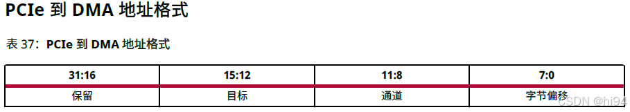
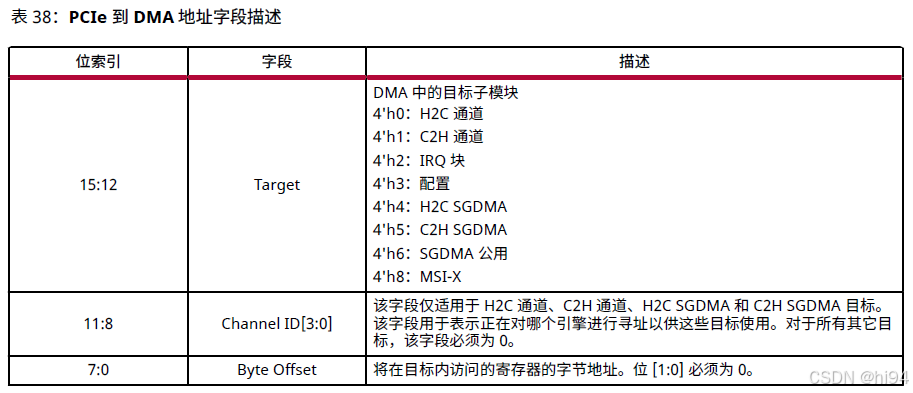
3.2.1 寄存器地址格式
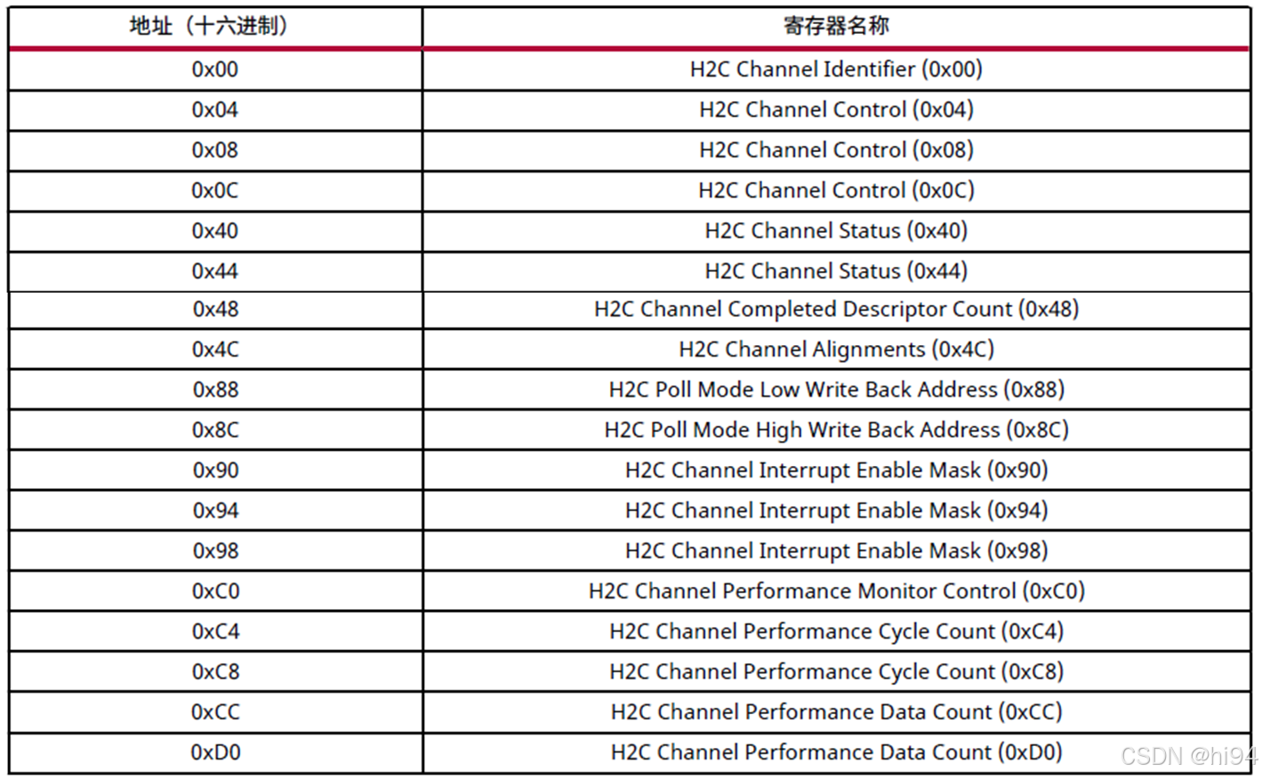
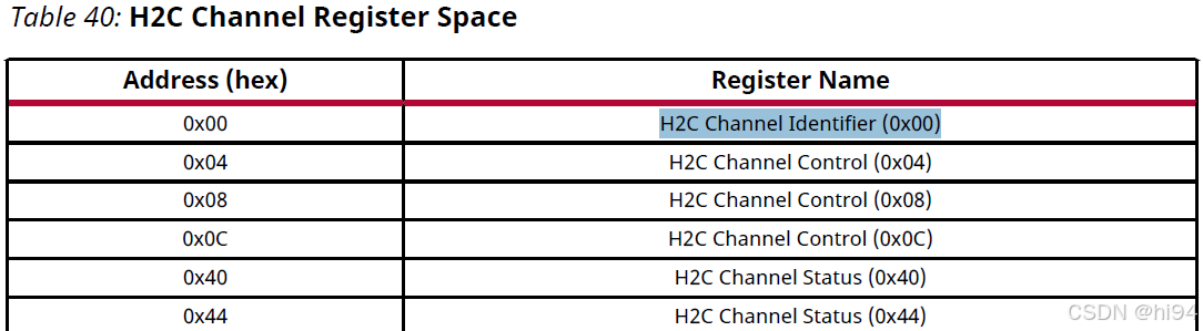
3.2.2 H2C 通道寄存器空间
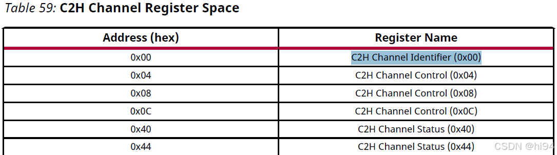
3.2.3 C2H 通道寄存器空间
3.2.4 其他寄存器空间
3.2.5 举例
4. Driver
4.1 PCIe 一些概念
4.1.1 BAR
4.1.2 中断与轮询
4.2 DMA drivers
4.2.1 PCIe Device IDs
4.2.2 编译并加载驱动
4.2.3 查看驱动信息
4.2.4 获取通道标识符
4.2.5 xdma0_user 测试
4.2.6 xdma0_bypass 测试
4.2.7 xdma0_h2c_0 读写测试
4.3 调试方法
4.3.1 xdma cdev init
4.3.2 h2c status
4.3.3 xfer timed out
4.3.4 Debug Options
4.3.5 信号完整性问题
5. 总结
1. 简介
1.1 Data Mover
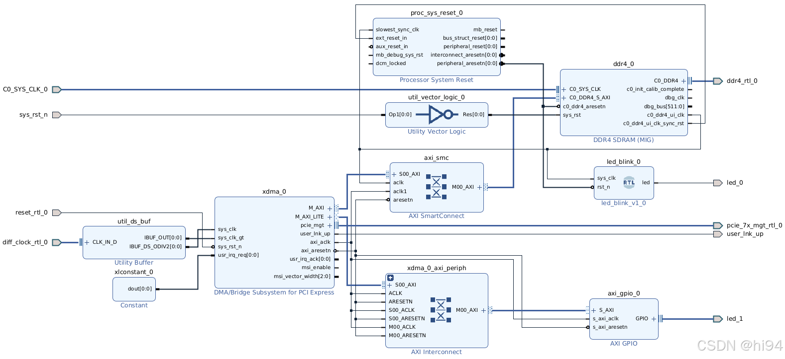
DMA/Bridge Subsystem for PCIe 就是一个数据搬运器件,用于在主机内存和 DMA 子系统之间搬运数据。子系统通过处理一种叫做 “描述符” 的数据结构来完成在主机内存和 DMA 子系统之间移动数据的任务。
|------|            |------------------------------FPGA-----------------------------|
|      |            |    |---------------|                  |-------------------|   |
|      |            |    |               |                  |                   |   |
| Host |    PCIe    |    |   DMA/Bridge  | M_AXI      S_AXI |   User Logic      |   |
| App  |<---------->|<-->|   for PCIe    |<---------------->|   e.g.            |   |
|      |    slot    |    |               |                  |   HW Accelerator  |   |
|      |            |    |  (AXI-master) |                  |   (AXI-slave)     |   |
|      |            |    |---------------|                  |-------------------|   |
|------|            |---------------------------------------------------------------|
连接不同的 AXI-slave,可以实现不同的功能:
- 连接 AXI BRAM 或 AXI DDR MC,则整个 FPGA 可以看作一个 PCIe 内存设备,Host-PC 可以读写该内存;
- 一个硬件加速器,则 Host-PC 可以通过 PCIe 调用该加速器;
- AXI 桥,下游挂多个 AXI slave ,可以同时实现更多功能。
1.2 描述符
你可以把 “描述符” 想象成一个包含了数据传输指令的小包裹。这个包裹里面明确地写着:
- 源 (Source): 数据从哪里来(例如,主机内存中的某个具体地址)。
- 目标 (Destination): 数据要到哪里去(例如,DMA 子系统中的某个地址,或者反过来)。
- 要传输数据量 (Amount of data to transfer): 需要移动多少数据(例如,多少个字节)。
DMA 子系统会读取并执行这些 “描述符” 中的信息,从而自动地将数据从源地址搬运到目标地址,而不需要 CPU 的直接干预。
简单来说,DMA 子系统依靠这些 “描述符” 来了解它需要做什么样的数据搬运工作。
2. ZCU102
2.1 Ubuntu OS
Install Ubuntu on AMD | Ubuntu Use Ubuntu on AMD for the familiar developer experience and an accelerated path to production.![]() https://ubuntu.com/download/amd
https://ubuntu.com/download/amd
2.2 USB Host
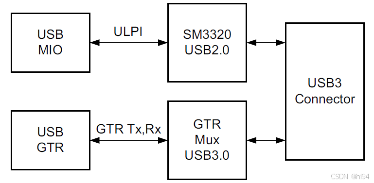
2.2.1 连接拓扑
PHY IC: USB3320 @U116
2.2.2 设备类型
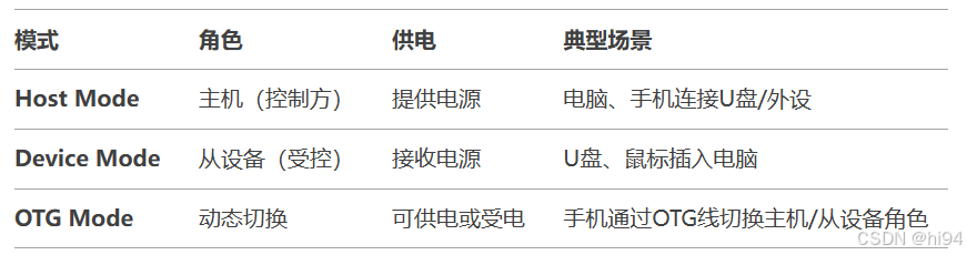
USB 设备类型
- A 类设备:指的是标准的 USB Host 设备,如计算机或笔记本电脑,它们提供电源并管理连接的 USB 设备。
- B 类设备:通常是外围设备,如打印机、鼠标或键盘,它们从 A 类设备接收电源和数据。
2.2.3 USB 跳帽设置
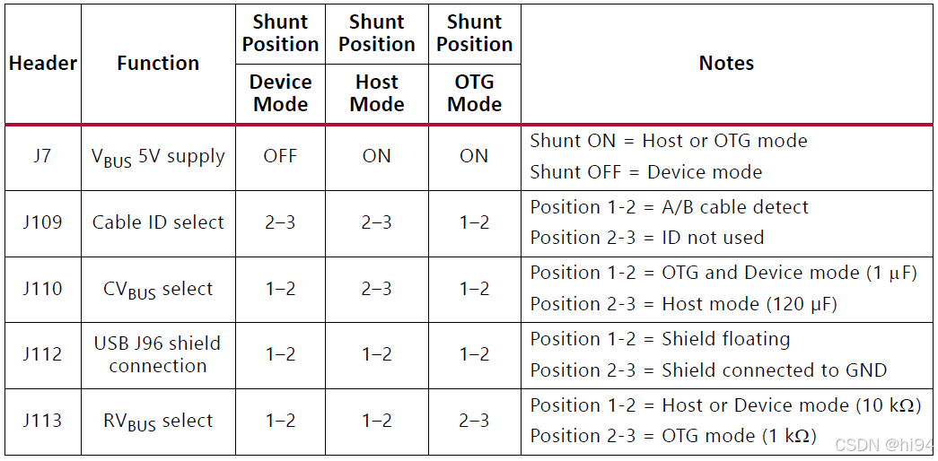
跳帽设置:

2.3 无线网卡

下载地址:
W311MI _Tenda-All For Better NetWorkingW311MI![]() https://www.tendacn.com/product/overview/W311MIv6.html
https://www.tendacn.com/product/overview/W311MIv6.html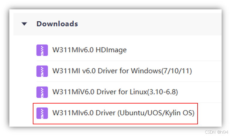
W311MIv6.0 Driver (Ubuntu/UOS/Kylin OS) 可以给 KV260、ZCU102 的 Ubuntu 系统使用。
2.4 PCIe Info
2.4.1 Diagram
1)Diagram
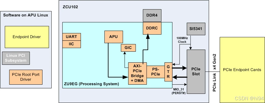
Form factor for PCIe Gen2x4 Host, Micro-ATX chassis footprint
2.4.2 lspci -tv
显示了系统的PCIe拓扑结构
>> lspci -tv
---
-[0000:00]---00.0-[01-0c]----00.0  Xilinx Corporation Device 9021
1)[0000:00]:是 PCIe 层级结构的根节点(Root Complex)
- 0000 是 PCI 域号(domain number),通常为 0000
- 00 是总线号(bus number),00 表示这是根总线
2)---00.0:是根端口(Root Port)的设备号和功能号
- 00 是设备号(device number)
- .0 是功能号(unction number)
3)-[01-0c]:表示这个根端口连接的下游设备所在的总线范围
- 01-0c 表示总线号从 01 到 0c (十进制12)
- 这意味着这个根端口下可以有多达 12 个不同的总线
4)00.0 Xilinx Corporation Device 9021
- 00.0 是子 PCI 设备的设备和功能编号
- Xilinx Corporation Device 9021 是设备的供应商和型号
>> lspci -vt
-[0000:00]-+-00.0  Intel Corporation Device 9b53+-01.0-[01]----00.0  Xilinx Corporation Device 9021+-02.0  Intel Corporation Device 9bc8+-04.0  Intel Corporation Xeon E3-1200 v5/E3-1500 v5/6th Gen Core Processor Thermal Subsystem+-12.0  Intel Corporation Comet Lake PCH Thermal Controller+-14.0  Intel Corporation Comet Lake USB 3.1 xHCI Host Controller+-14.2  Intel Corporation Comet Lake PCH Shared SRAM+-16.0  Intel Corporation Comet Lake HECI Controller+-16.3  Intel Corporation Device 06e3+-17.0  Intel Corporation Device 06d2+-1b.0-[02]----00.0  SK hynix Device 1339+-1f.0  Intel Corporation Device 0687+-1f.3  Intel Corporation Comet Lake PCH cAVS+-1f.4  Intel Corporation Comet Lake PCH SMBus Controller+-1f.5  Intel Corporation Comet Lake PCH SPI Controller\-1f.6  Intel Corporation Ethernet Connection (11) I219-LM
这两行:
+-01.0-[01]----00.0 Xilinx Corporation Device 9021
+-1b.0-[02]----00.0 SK hynix Device 1339
这两行之所以看起来和别的不一样,它们表示的是 PCI 桥(PCI Bridge) 以及连接在该桥后面的设备。
- 普通行 (例如 +-02.0 Intel Corporation Device 9bc8): 显示的是直接连接在当前总线(这里是总线 00)上的终端设备(Endpoint Device),比如集成显卡、USB 控制器、网卡等。它们不连接其它总线。
- 特殊行 (例如 +-01.0-[01]----00.0 Xilinx ...): 显示的是一个 PCI 桥 (01.0) 以及通过这个桥连接到下一级(次级)总线 ([01]) 上的第一个设备 (00.0)。这种表示方法突出了设备间的层级和连接关系,显示了哪些设备是挂载在桥下面的。
2.4.3 lspci -v
lspci 提供了系统中 PCIe 桥接设备(Xilinx Corporation 制造)的详细信息:
ubuntu@zynqmp:~$ lspci -vv
---
00:00.0 PCI bridge: Xilinx Corporation Device d021 (prog-if 00 [Normal decode])Control: I/O- Mem- BusMaster+ SpecCycle- MemWINV- VGASnoop- ParErr- Stepping- SERR- FastB2B- DisINTx-Status: Cap+ 66MHz- UDF- FastB2B- ParErr- DEVSEL=fast >TAbort- <TAbort- <MAbort- >SERR- <PERR- INTx-Latency: 0Interrupt: pin A routed to IRQ 62Bus: primary=00, secondary=01, subordinate=0c, sec-latency=0I/O behind bridge: 00000000-00000fff [size=4K]Memory behind bridge: [disabled]Prefetchable memory behind bridge: [disabled]Secondary status: 66MHz- FastB2B- ParErr- DEVSEL=fast >TAbort- <TAbort- <MAbort- <SERR- <PERR-BridgeCtl: Parity- SERR+ NoISA- VGA- VGA16- MAbort- >Reset- FastB2B-PriDiscTmr- SecDiscTmr- DiscTmrStat- DiscTmrSERREn-Capabilities: <access denied>Kernel driver in use: pcieport
2.4.2.1 设备基本信息
1)设备位置与类型
- 00:00.0 表示设备在 PCI 总线上的位置(总线 00,设备 00,功能 0)。
- 这是一个 PCI 桥接器(PCI bridge),型号为 Xilinx Corporation Device d021,用于连接主总线(00)和次级总线(01-0c)。
2)编程接口(prog-if)
- Normal decode 表示桥接器以标准方式解码 PCI 地址。
2.4.2.2 控制与状态寄存器
- 功能禁用(带
-),功能启用(带+)
1)Control 寄存器
- BusMaster+:桥接器可以发起总线请求(DMA 操作)。
- I/O- Mem-:桥接器未启用 I/O 和内存空间访问(可能未配置或未激活)。
- 其他标志(如 SERR-、FastB2B-)表示错误报告和快速传输功能未启用。
2)Status 寄存器
- Cap+:设备支持 Capability List(扩展功能列表)。
- DEVSEL=fast:设备快速响应访问请求。
- 无错误状态(ParErr-、SERR- 等)。
2.4.2.3 中断与总线拓扑
1)中断路由:
- Interrupt: pin A routed to IRQ 62
- 桥接器的中断引脚 A 连接到系统的 IRQ 62。
2)总线范围:
- primary=00:主总线编号 00(连接 CPU)。
- secondary=01:次级总线起始编号 01。
- subordinate=0c:次级总线结束编号 0c(表示该桥接器下可管理总线 01-0c)。
- sec-latency=0:次级总线访问延迟为 0。
2.4.2.4 地址空间配置
1)I/O 空间:
- 00000000-00000fff [size=4K]
- 桥接器后挂载的设备的 I/O 空间范围为 4KB,但当前未启用(I/O behind bridge 未分配实际地址)。
2)内存空间:
- Memory behind bridge: [disabled]
- 内存和预取内存空间均未启用(可能需动态配置或未使用)。
2.4.2.5 桥接器控制与能力
1)Secondary Status
- 次级总线的状态(类似主状态寄存器),无错误或特殊配置。
2)BridgeCtl
- 控制桥接器行为的标志,例如:
- SERR+:启用系统错误报告。
- NoISA-:允许 ISA 风格的访问(已过时)。
- VGA-:不支持 VGA 兼容模式。
3)Capabilities:
- <access denied> 表示需要 root 权限才能查看扩展功能(如 PCIe 链路速度、电源管理等)。
2.4.2.6 内核驱动
- Kernel driver in use: pcieport
当前由 Linux 内核的 pcieport 驱动管理,该驱动负责处理 PCIe 端口和桥接器的通用功能(如热插拔、错误处理等)。
2.4.4 setpci
1)COMMAND 寄存器
在 PCIe 设备中,COMMAND 寄存器是一个 16位寄存器,控制设备的基本操作权限,其低 8 位的标志位控制设备的核心功能:
Bit 	Name            Function
--------------------------------------------------------------------------------
0       I/O Space       启用设备对 I/O 端口 的访问(如 in/out 指令)
1       Memory Space    启用设备对 内存映射寄存器(MMIO) 的访问(如 BAR0/BAR1)
2       Bus Mastering   允许设备发起 DMA 操作(直接读写主机内存)
3-15	Others          如中断禁用、快速背靠背传输等(通常次要)
2)查看 Control 状态
>> sudo lspci -vv -s 01:00.0 | grep Control
---
Control: I/O- Mem- BusMaster- SpecCycle- MemWINV- VGASnoop- ParErr- Stepping- SERR- FastB2B- DisINTx-
说明当前设备 所有关键功能均未启用,无法访问它的内存或寄存器。
3)启用功能
>> sudo setpci -s 01:00.0 COMMAND=0x070x07 的二进制是 00000111,它同时启用:
- Bit 0 (I/O Space) = 1 → 允许 I/O 访问
- Bit 1 (Memory Space) = 1 → 允许 MMIO 访问
- Bit 2 (Bus Mastering) = 1 → 允许 DMA
为什么内核没有自动启用?
- 无专用驱动加载:内核检测到设备但未绑定驱动时,可能不会主动启用其功能。
- 安全策略限制:部分系统默认禁用未认证设备的 Bus Mastering(防 DMA 攻击)。
4)查看驱动加载情况
>> sudo dmesg | grep 9021
---
[    3.807355] pci 0000:01:00.0: [10ee:9021] type 00 class 0x058000
从 dmesg 输出和之前的 lspci 信息来看,并没有为这个 Xilinx 设备(9021)加载专用驱动。
2.4.5 命令汇总
| 用途 | 命令 |
| 快速查看设备 | lspci |
| 查看详细信息 | lspci -vv |
| 查看拓扑结构 | lspci -tv |
| 查找 Xilinx 设备 | lspci -d 10ee |
| 检查 PCIe 链路 | lspci -vv | grep -i "width|speed" |
| 查看内存映射 | lspci -v | grep -i memory |
| 检查驱动绑定 | lspci -k |
>> lspci
---
00:00.0 PCI bridge: Xilinx Corporation Device d021
命名规则
<bus>:<device>.<function>
- 1. <bus> - 01,总线号(Bus Number) 。这里是 00,表示该设备连接到总线 0。
- 2. <device> - 00,设备号(Device Number) 。这里是 00,表示这是总线 0 上的第 1 个设备(设备号从 0 开始)。
- 3. <function> - 0,功能号(Function Number) 。这里是 0,表示这是该设备的第 1 个功能(功能号从 0 开始)。
3. ZCU102+KU5P
3.1 vivado 工程
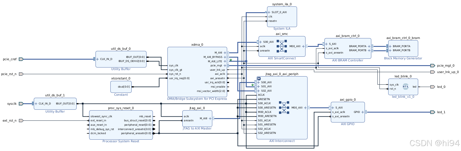
3.1.1 Block Design
1)PCIe BRAM
XDC:
set_property IOSTANDARD LVCMOS33 [get_ports led_0]
set_property PACKAGE_PIN J12     [get_ports led_0]set_property PACKAGE_PIN H14     [get_ports {led_1_tri_io[0]}]
set_property IOSTANDARD LVCMOS33 [get_ports {led_1_tri_io[0]}]set_property PACKAGE_PIN H12     [get_ports user_lnk_up_0]
set_property IOSTANDARD LVCMOS33 [get_ports user_lnk_up_0]set_property PACKAGE_PIN V7 [get_ports {pcie_cref_clk_p[0]}]set_property PACKAGE_PIN T19     [get_ports pcie_rst_n]
set_property IOSTANDARD LVCMOS18 [get_ports pcie_rst_n]set_property PACKAGE_PIN K22        [get_ports {sysclk_clk_p[0]}]
set_property IOSTANDARD DIFF_SSTL12 [get_ports {sysclk_clk_p[0]}]set_property PACKAGE_PIN J14     [get_ports ext_rst_n]
set_property IOSTANDARD LVCMOS33 [get_ports ext_rst_n]create_clock -period 10.000 -name {pcie_cref_clk_p[0]} -waveform {0.000 5.000} [get_ports {pcie_cref_clk_p[0]}]set_property BITSTREAM.GENERAL.COMPRESS TRUE  [current_design]
set_property BITSTREAM.CONFIG.CONFIGRATE 51.0 [current_design]
set_property BITSTREAM.CONFIG.SPI_BUSWIDTH 4  [current_design]
set_property CONFIG_MODE SPIx4 [current_design]
set_property C_CLK_INPUT_FREQ_HZ 300000000 [get_debug_cores dbg_hub]
set_property C_ENABLE_CLK_DIVIDER false    [get_debug_cores dbg_hub]
set_property C_USER_SCAN_CHAIN 1           [get_debug_cores dbg_hub]
connect_debug_port dbg_hub/clk [get_nets clk]
2)PCIe DDR
XDC 参见:
《 Vivado - JTAG to AXI Master (DDR4初始化读写测试)-CSDN博客 》
3.1.2 IBUFDS_GTE
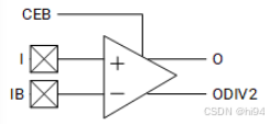
Primitive: Gigabit Transceiver Buffer
对于高速 GT,需要使用 IBUFDS_GTE,如果使用 IBUFDS,在编译或者生成 bit 时会报错,提示该时钟约束有问题。
3.1.3 XDMA PCIe
IP: DMA/Bride Subsystem for PCI Express v4.1
1)Basic Tab
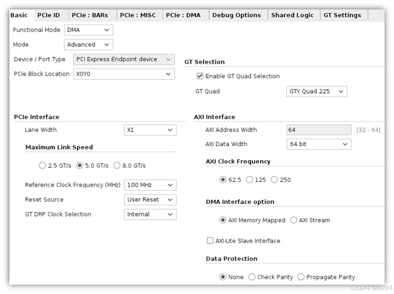
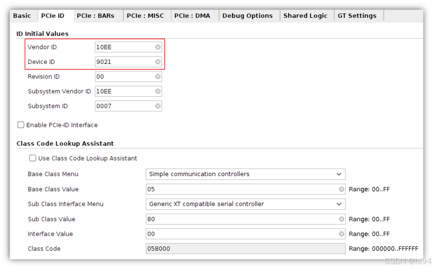
2)PCIe ID Tab
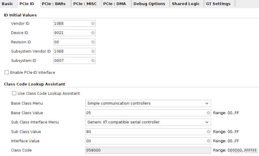
Device ID(9021)含义:
- 9 - Ultrascale+ 系列
- 2 - PCIe 2.0(5Gbps)
- 1 - 通信链路 Lane = 1
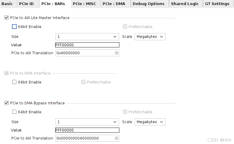
3)PCIe:BARs Tab
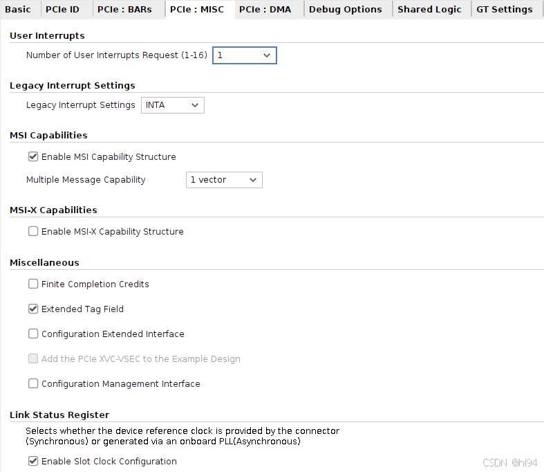
4)PCIe:MISC Tab
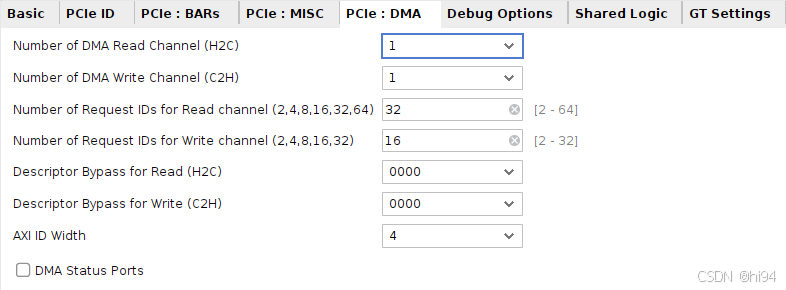
5)PCIe:DMA Tab
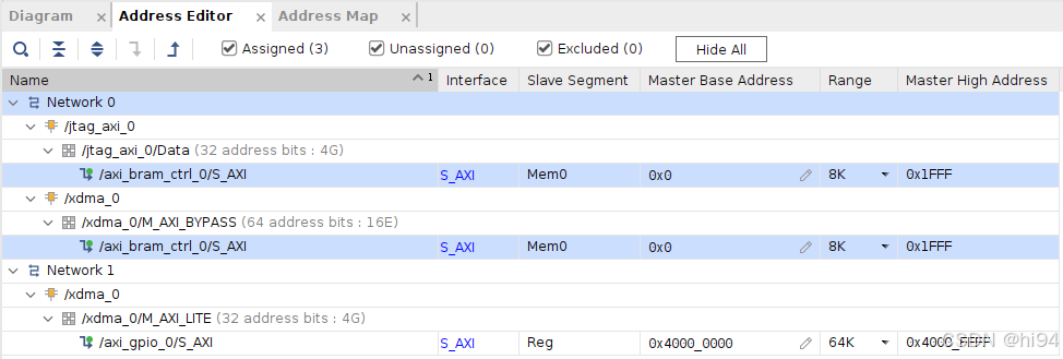
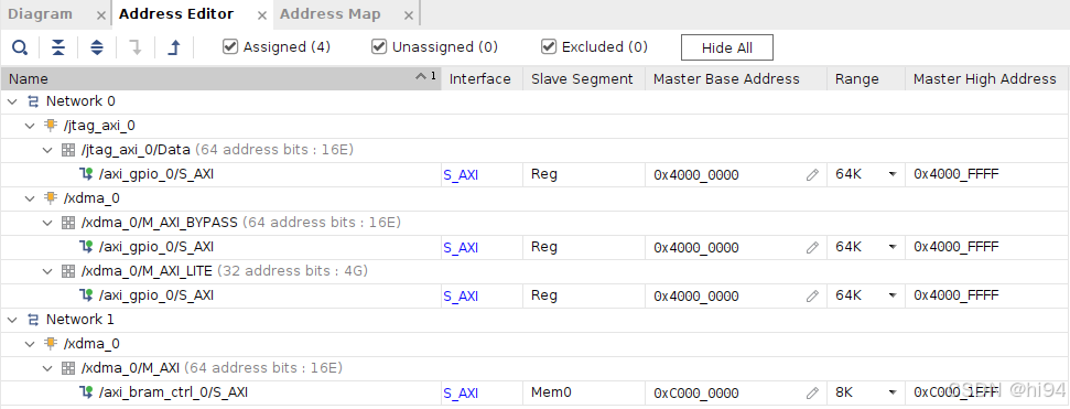
3.1.4 Address Editor
3.1.5 烧写与固化
1)生成 bin 文件的相关配置
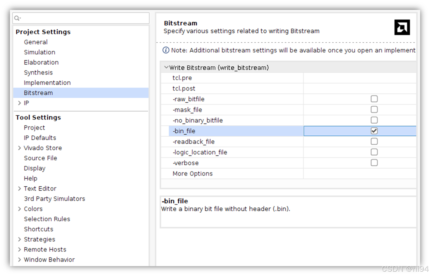
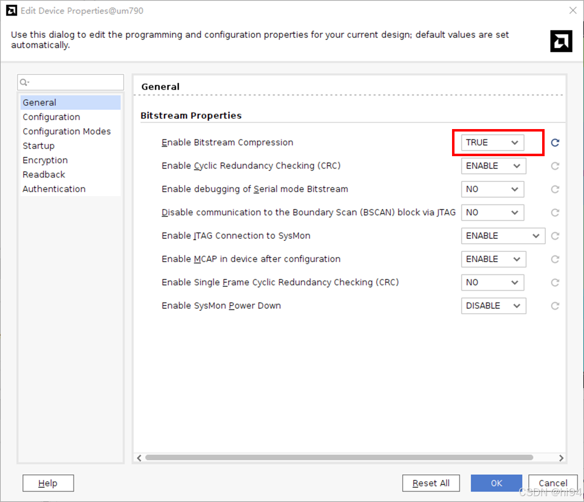
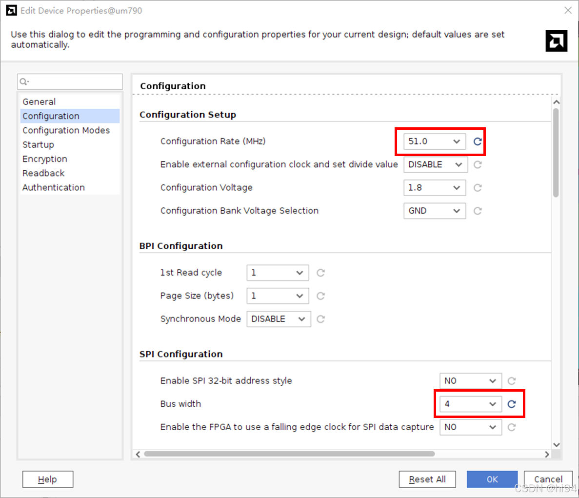
2) 配置 BITSTREAM 属性
直接添加 XDC 约束:
set_property BITSTREAM.GENERAL.COMPRESS     TRUE  [current_design]
set_property BITSTREAM.CONFIG.CONFIGRATE    51.0  [current_design]
set_property BITSTREAM.CONFIG.SPI_BUSWIDTH  4     [current_design]
或者通过 GUI 配置:
打开综合后或实现后的设计,Tools -> Edit Device Properties:
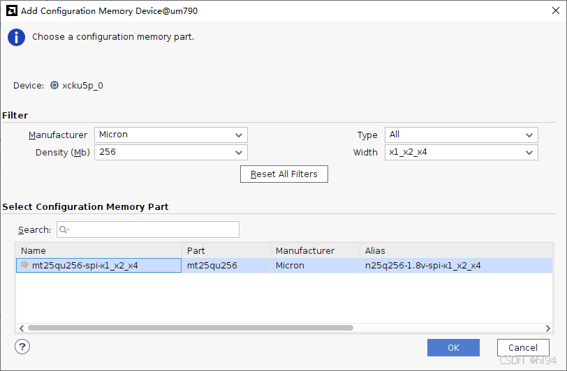
3)添加 Flash 设备
4)执行烧写
3.2 寄存器空间
3.2.1 寄存器地址格式
DMA/Bridge Subsystem for PCIe 寄存器可从主机或 AXI 从接口进行访问。这些寄存器应用于 DMA 编程和状态检查。
3.2.2 H2C 通道寄存器空间
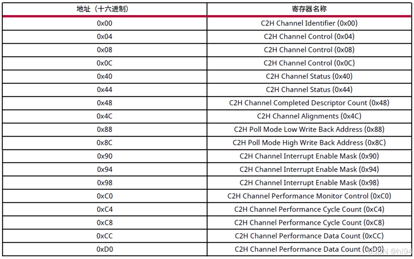
3.2.3 C2H 通道寄存器空间
3.2.4 其他寄存器空间
3.2.5 举例
1)地址 0x0000_0040
表示 H2C 类别中,第一个通道,H2C Channel Status (0x40) 寄存器
2)地址 0x0000_1040
表示 C2H 类别中,第一个通道,H2C Channel Status (0x40) 寄存器
3)地址 0x0000_1100
表示 C2H 类别中,第二个通道,H2C Channel Identifier (0x00) 寄存器
4)0x0000_3000
表示配置块寄存器 (0x3)中,Config Block Identifier (0x00) 寄存器
4. Driver
4.1 PCIe 一些概念
4.1.1 BAR
1)BAR的基本含义
BAR(Base Address Register)
BAR 是 PCIe 设备用来定义其内存空间或 I/O 空间在系统地址空间中的基地址(Base Address)的寄存器。每个 BAR 会映射到一个物理地址范围,系统通过这个范围访问设备的资源(如内存、寄存器等)。
BAR 的大小和类型(内存空间或I/O空间)由 BAR 的配置决定。
在 PCIe 设备中,通常有多个 BAR(例如,6个BAR),每个 BAR 可以独立配置。
2)BAR的作用
BAR 的用途是为 PCIe 设备提供一种与主机(Host)通信的机制:
内存空间映射:通过 BAR,操作系统或驱动程序可以访问 FPGA 内部的内存或寄存器。
地址分配:在系统启动时,BIOS 或操作系统会为每个 BAR 分配一个唯一的物理地址。
设备功能支持:不同的 BAR 可以用于不同的功能,例如数据传输、控制寄存器访问等。
4.1.2 中断与轮询
1)切换为轮询
默认情况下,驱动程序使用中断来通知 DMA 传输完成。如何修改驱动程序以使用轮询而不是中断来确定 DMA 事务何时完成?
答:在插入内核模块时,可以将驱动程序从中断驱动(默认)更改为轮询驱动(轮询模式)。
sudo ./load_driver.sh 4
---
interrupt_selection 4.
xdma                   98304  0
Loading driver...insmod xdma.ko poll_mode=1 ...The Kernel module installed correctly and the xmda devices were recognized.
DONE
注意:中断模式与轮询模式将应用于所有 DMA 通道。如果需要,可以修改驱动程序,使某些通道为中断驱动,而其他通道为轮询驱动。有关在轮询模式下使用 PCIe DMA IP 的更多信息,请参阅 PG195 中的轮询模式部分。
2)中断
中断需要周密的思考和规划,因为它们在设备驱动程序中扮演着关键角色。中断处理可能具有挑战性,因为它们需要大量测试来验证没有问题;而当问题出现时(例如中断丢失),调试起来可能非常困难。包含大量调试代码的 Linux 驱动程序可能会改变其行为,以至于操作完全失效,或者运行极其缓慢,从而严重改变系统状态。
有些中断是电平触发(level triggered),有些中断是边沿触发(edge triggered)。这些中断会被转换为 PCIe 中断。PCIe IP 的中断输入因具体 IP 而异,但通常是一个请求(request)随后跟一个许可(grant),表示该 IP 已接受请求。可能需要进行一些从 IP 中断到 PCIe 中断的转换。AXI IIC IP 核是电平触发中断,而 AXI QSPI IP 核是边沿触发中断。对于电平触发中断,应在驱动程序中仔细检查,以确保根据从 IP 域到 PCIe 域的转换方式,中断不会丢失。
在文档中查找 IP 的中断触发类型可能很有挑战性,但可以在 Vivado 中查看,如下所示。选中中断引脚(interrupt pin),然后查看其配置,即可看到信号的敏感度(sensitivity)(边沿或电平)。
3)整体思路
在主机 CPU 上运行的 DMA 驱动程序的目的是准备外设的 DMA 传输,因为只有操作系统(OS)才完全控制着内存系统、文件系统以及用户空间进程。首先,需要对外设的 DMA 引擎进行编程,设置要复制的内存范围的源地址和目标地址。其次,通知设备开始 DMA 传输。当传输完成时,设备通常会产生中断,以通知 CPU 传输已结束。对于每个中断,一个由驱动程序预先安装的中断处理程序会被调用,然后操作系统可以相应地确认已完成的传输。
4.2 DMA drivers
4.2.1 PCIe Device IDs
如何修改内核模块驱动识别的 PCIe 设备 ID?
参见 "dma_ip_drivers-master\XDMA\linux-kernel\readme.txt"
xdma/xdma_mod.c 文件中包含 pci_device_id 结构体,用于识别驱动支持的 PCIe 设备 ID,格式如下:
//        Vendor ID, Device ID
{ PCI_DEVICE(0x10ee, 0x9021), },
根据需要添加、删除或修改此结构体中的 PCIe Device ID。然后卸载现有的 xdma 内核模块,重新编译驱动,并使用 load_driver.sh 脚本重新安装驱动。
4.2.2 编译并加载驱动
1)编译 KO 模块
>> cd <dma_ip_drivers-master>/XDMA/linux-kernel/xdma/
>> sudo make install
在 xdma 路径下创建了两个文件:xdma.mod.o、xdma.ko
-rw-rw-r-- 1 dd dd 4769480 April   4 17:22 xdma.ko
-rw-rw-r-- 1 dd dd 126880  April   4 17:22 xdma.mod.o
2)编译测试工具(tools)
>> cd <dma_ip_drivers-master>/XDMA/linux-kernel/tools
>> make
会出现一些 warning,可以忽略。
3)加载内核模块驱动程序,有两种方法:
- 通过 shell 命令直接加载
modprobe xdma通过 script
>> sudo ./load_driver.sh
---
interrupt_selection .
xdma                   98304  0
Loading driver...insmod xdma.ko interrupt_mode=2 ...The Kernel module installed correctly and the xmda devices were recognized.
DONE
4.2.3 查看驱动信息
1)加载驱动后
>> sudo lspci -vv -s 01:00.0 | grep Kernel
---
Kernel driver in use: xdma
Kernel modules: xdma
2)对应的设备节点
>> ll /dev/xdma*
---
/dev/xdma0_control
/dev/xdma0_h2c_0
/dev/xdma0_c2h_0
/dev/xdma0_bypass
/dev/xdma0_bypass_h2c_0
/dev/xdma0_bypass_c2h_0
/dev/xdma0_user
/dev/xdma0_xvc/dev/xdma0_events_0
/dev/xdma0_events_1
...
/dev/xdma0_events_15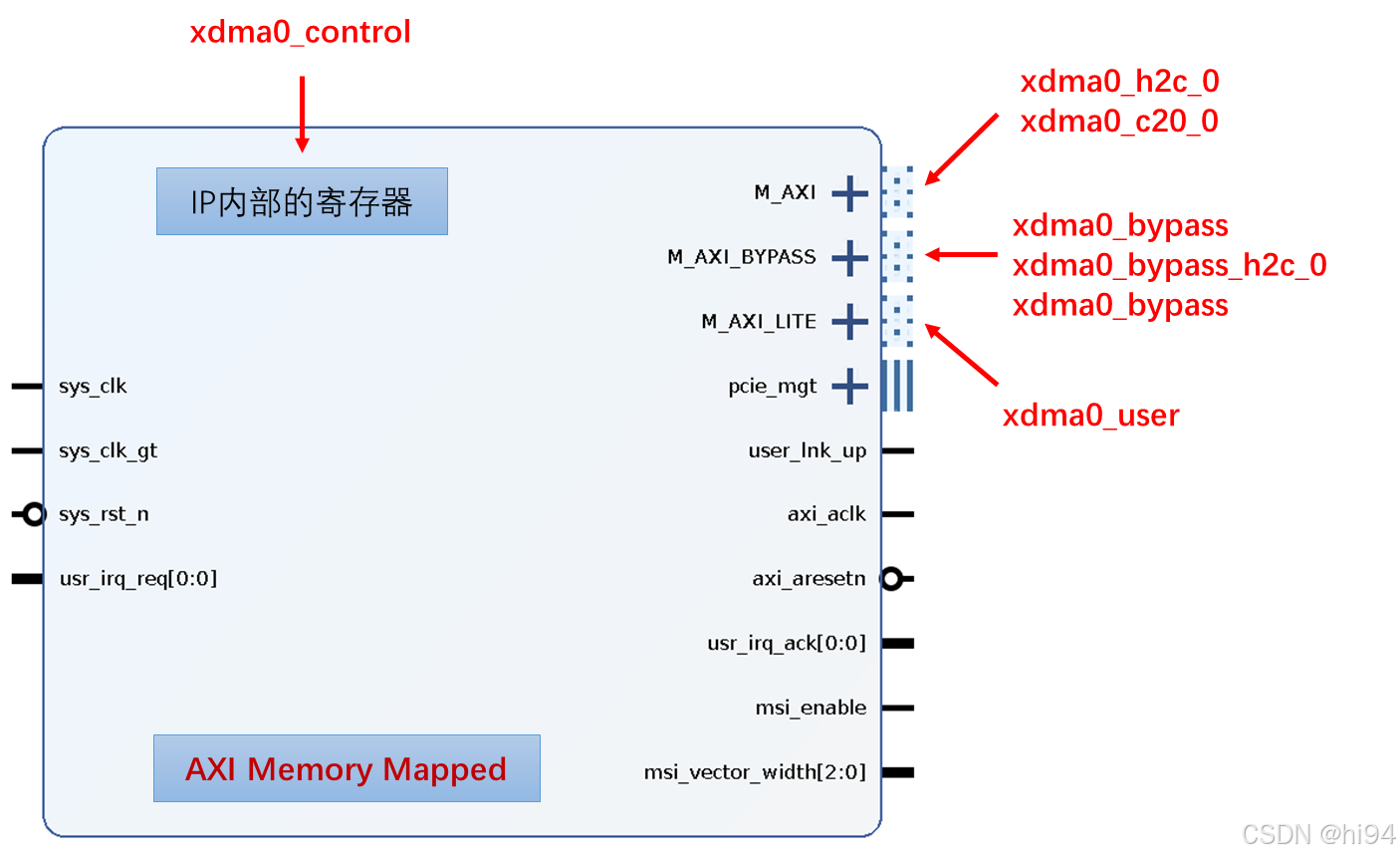
3)查看驱动程序详情
PS:无需指定路径
>> modinfo xdma
---
filename:       /lib/modules/5.15.0-126-generic/xdma/xdma.ko
license:        Dual BSD/GPL
version:        2020.2.2
description:    Xilinx XDMA Reference Driver
author:         Xilinx, Inc.
srcversion:     2EEB4A2EC40A3FC02ABA554
alias:          pci:v00001D0Fd0000F001sv*sd*bc*sc*i*
alias:          pci:v00001D0Fd0000F000sv*sd*bc*sc*i*
alias:          pci:v000010EEd00002808sv*sd*bc*sc*i*
...
...
depends:
retpoline:      Y
name:           xdma
vermagic:       5.15.0-126-generic SMP mod_unload modversions
parm:           h2c_timeout:H2C sgdma timeout in seconds, default is 10 sec. (uint)
parm:           c2h_timeout:C2H sgdma timeout in seconds, default is 10 sec. (uint)
parm:           poll_mode:Set 1 for hw polling, default is 0 (interrupts) (uint)
parm:           interrupt_mode:0 - Auto , 1 - MSI, 2 - Legacy, 3 - MSI-x (uint)
parm:           enable_st_c2h_credit:Set 1 to enable ST C2H engine credit feature, default is 0 ( credit control disabled) (uint)
parm:           desc_blen_max:per descriptor max. buffer length, default is (1 << 28) - 1 (uint)
4.2.4 获取通道标识符
通过 Channel Identifier(通道标识符),可以得到通道属性:
- Channel exist
- Channel Target(H2C / C2H)
- Stream / Mem map
- Channel ID
- Version
1)发送通道查询指令
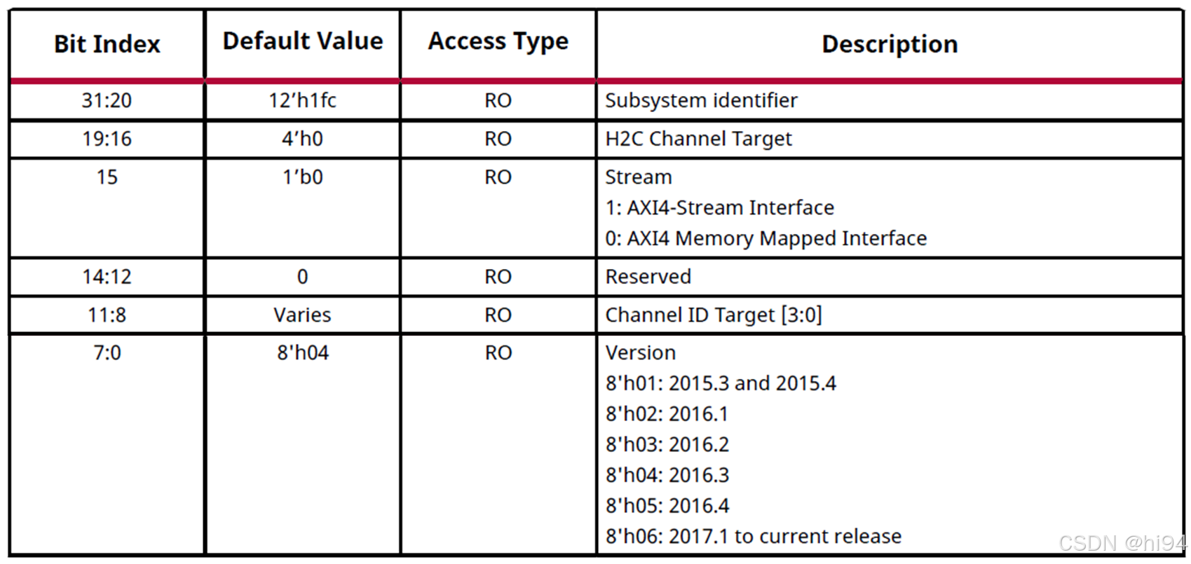
>> sudo ./reg_rw /dev/xdma0_control 0x0000设备节点 /dev/xdma0_control 的寄存器描述《pg195-pcie-dma-en-us-4.1》:
|-----------|----------------|------------------------------------------------------------|
| Bit Index | Field          | Description                                                |
|-----------|----------------|------------------------------------------------------------|
| 15:12     | Target         | The destination submodule within the DMA                   |
|           |                | 4'h0: H2C Channels                                         |
|           |                | 4'h1: C2H Channels                                         |
|           |                | 4'h2: IRQ Block                                            |
|           |                | 4'h3: Config                                               |
|           |                | 4'h4: H2C SGDMA                                            |
|           |                | 4'h5: C2H SGDMA                                            |
|           |                | 4'h6: SGDMA Common                                         |
|           |                | 4'h8: MSI-X                                                |
|-----------|----------------|------------------------------------------------------------|
| 11:8      | Channel ID[3:0]| This field is only applicable for H2C Channel, C2H Channel,|
|           |                | H2C SGDMA, and C2H SGDMA Targets. This field indicates     |
|           |                | which engine is being addressed for these Targets.         |
|           |                | For all other Targets this field must be 0.                |
|-----------|----------------|------------------------------------------------------------|
| 7:0       | Byte Offset    | The byte address of the register to be accessed within the |
|           |                | target. Bits[1:0] must be0.                                |
|-----------|----------------|------------------------------------------------------------|
例一,向 /dev/xdma0_control 写入 0x0000 时,表示查询 H2C 的第一个通道 identifier 信息:
- Target[15:12]: 0x0 - H2C Channels
- Channel[11:8]: 0x0 - No 1.
- ByteOffset[7:0]: 0x00 - Channel Identifier (0x00)
例二,向 /dev/xdma0_control 写入 0x1003 时,表示查询 C2H 第四个通道 identifier 信息:
- Target[15:12]: 0x0 - C2H Channels
- Channel[11:8]: 0x0 - No 4.
- ByteOffset[7:0]: 0x00 - Channel Identifier (0x00)
例三,向 /dev/xdma0_control 写入 0x0040 时,表示查询 H2C 的第一个通道 identifier 信息:
- Target[15:12]: 0x0 - H2C Channels
- Channel[11:8]: 0x0 - No 1.
- ByteOffset[7:0]: 0x40 - Channel Status (0x40)
2)回读信息解释
>> sudo ./reg_rw /dev/xdma0_control 0x0000
---
device: /dev/xdma0_control, address: 0x0 (0x0+0x0), access read.
access width: word (32-bits)
character device /dev/xdma0_control opened.
Memory 0x0 mapped at address 0x7f924a39c000.
Read 32-bit value at address 0x0 (0x7f924a39c000): 0x1fc00006
返回值 0x1fc10006 表示:
- [31:20]: 12’h1fc - DMA Subsystem,该通道启用,否则读出 0
- [19:16]: 4'h0 - H2C Channels
- [15]: 1'b0 - AXI4 Memory Mapped Interface
- [11:8]: 4'h0 - Channel 1
- [7:0]: 8'h06 - 2017.1 to current release
《pg195-pcie-dma-en-us-4.1》
4.2.5 xdma0_user 测试
1)写入设备节点 /dev/xdma0_user,地址为 0x4,数据为 0x0。
- 设备节点 /dev/xdma0_user 可以理解为 基地址,由 Host 分配。
- 地址 0x4 可以理解为 偏移地址。
sudo ./reg_rw /dev/xdma0_user 0x4 w 0x0 # axi_gpio out
---
device: /dev/xdma0_user, address: 0x4 (0x0+0x4), access write.
access width: word (32-bits)
character device /dev/xdma0_user opened.
Memory 0x0 mapped at address 0x7fac3e7c0000.
Write 32-bits value 0x00000000 to 0x4 (0x0x7fac3e7c0004)
设备节点 /dev/xdma0_user 可访问的地址范围:
PCIe to AXI Translation        = 0x400000000
|
PCIe to AXI Translation + Size = 0x40000FFFF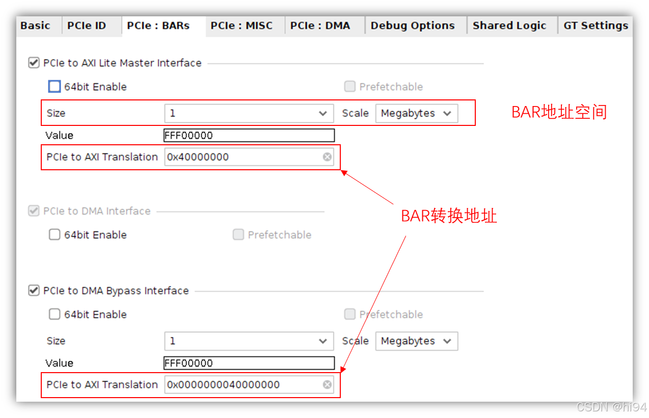
我们实际先要操作的寄存器地址是 0x40000004,如下图 Address Editor 所示:
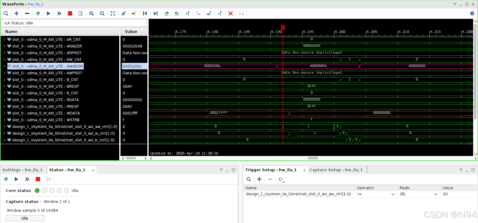
通过 ILA 查看实际传递到 M_AXI_LITE 的地址:
sudo ./reg_rw /dev/xdma0_user 0x0 w 0x1 # axi_gpio Highsudo ./reg_rw /dev/xdma0_user 0x0 w 0x0 # axi_gpio Low4.2.6 xdma0_bypass 测试
sudo ./reg_rw /dev/xdma0_bypass 0x4 w 0x0 # axi_gpio outsudo ./reg_rw /dev/xdma0_bypass 0x0 w 0x1 # axi_gpio Highsudo ./reg_rw /dev/xdma0_bypass 0x0 w 0x0 # axi_gpio Low4.2.7 xdma0_h2c_0 读写测试
sudo ./dma_from_device -d /dev/xdma0_c2h_0 -f ./output_datafile0_4K.bin -s 1024 -c 1 &sudo ./dma_to_device -d /dev/xdma0_h2c_0 -f ./datafile0_4K.bin -s 1024 -a 0 -c 1成功的标志:
>>sudo ./dma_to_device -d /dev/xdma0_h2c_0 -f ./datafile0_4K.bin -s 1024 -a 0 -c 1 -v
---
dev /dev/xdma0_h2c_0, addr 0x0, aperture 0x0, size 0x400, offset 0x0, count 1
host buffer 0x1400 = 0x557119548000
#0: CLOCK_MONOTONIC 0.000121792 sec. write 1024 bytes
** Avg time device /dev/xdma0_h2c_0, total time 121792 nsec, avg_time = 121792.000000, size = 1024, BW = 8.407777
/dev/xdma0_h2c_0 ** Average BW = 1024, 8.407777
4.3 调试方法
4.3.1 xdma cdev init
调查 ubuntu 启动时,关于 xdma 的 Log:
sudo dmesg | grep xdma
---
[    7.205815] xdma: loading out-of-tree module taints kernel.
[    7.222642] xdma: module verification failed: signature and/or required key missing - tainting kernel
[    7.224451] xdma:xdma_mod_init: Xilinx XDMA Reference Driver xdma v2020.2.2
[    7.224453] xdma:xdma_mod_init: desc_blen_max: 0xfffffff/268435455, timeout: h2c 10 c2h 10 sec.
[    7.226197] xdma:xdma_device_open: xdma device 0000:01:00.0, 0x00000000d756b14e.
[    7.226331] xdma:map_single_bar: BAR0 at 0xe1100000 mapped at 0x0000000063e767e1, length=1048576(/1048576)
[    7.226340] xdma:map_single_bar: BAR2 at 0xe1300000 mapped at 0x000000007347ea88, length=65536(/65536)
[    7.226344] xdma:map_bars: config bar 2, pos 1.
[    7.226349] xdma:map_single_bar: BAR4 at 0xe1200000 mapped at 0x0000000023370d3e, length=1048576(/1048576)
[    7.226351] xdma:identify_bars: 3 BARs: config 1, user 0, bypass 4.
[    7.228186] xdma:pci_keep_intx_enabled: 0000:01:00.0: clear INTX_DISABLE, 0x406 -> 0x6.
[    7.228245] xdma:probe_one: 0000:01:00.0 xdma0, pdev 0x00000000d756b14e, xdev 0x000000002e86ec3b, 0x00000000fc2eb3b5, usr 16, ch 1,1.
[    7.255484] xdma:cdev_xvc_init: xcdev 0x0000000045e9570d, bar 0, offset 0x40000.
日志关键信息的解读:
1)xdma: loading out-of-tree module taints kernel.
- 表明 xdma 模块正在被加载。它是一个 "out-of-tree" 模块(不是内核自带的),是另外编译安装的(非官方代码),加载这类模块会 "污染" (taint) 内核。
2)xdma:xdma_mod_init: Xilinx XDMA Reference Driver xdma v2020.2.2
- 驱动的初始化函数 xdma_mod_init 已经开始执行,并打印了驱动的版本号。
3)xdma:xdma_device_open: xdma device 0000:01:00.0, ...
- 成功检测到了一个 PCI 设备,其地址为 0000:01:00.0。
4)xdma:map_single_bar: BAR0 ... mapped ...
- 驱动成功映射了设备的 PCI BARs。
5)xdma:probe_one: 0000:01:00.0 xdma0, ...
- probe_one 函数成功完成了对设备 0000:01:00.0 的探测和初始化,并将其命名为 xdma0。
6)xdma:cdev_xvc_init: ...
- 其他初始化,创建字符设备接口 (cdev),用于用户空间程序与驱动交互。
4.3.2 h2c status
查询 H2C 的第一个通道 H2C Channel Status (0x40) 信息
>> sudo ./reg_rw /dev/xdma0_control 0x0040
---
access width: word (32-bits)
character device /dev/xdma0_control opened.
Memory 0x0 mapped at address 0x7f590b853000.
Read 32-bit value at address 0x40 (0x7f590b853040): 0x00000001
4.3.3 xfer timed out
发起 DMA 传输
sudo ./dma_to_device -d /dev/xdma0_h2c_0 -f ./datafile0_4K.bin -s 512 -a 0 -c 1
---
/dev/xdma0_h2c_0, write 0x200 @ 0x0 failed -1.
write file: Unknown error 512
查看调试信息
sudo dmesg | grep xdma
---
[   83.849094] xdma:xdma_xfer_submit: xfer 0x00000000a31d2506,512, s 0x1 timed out, ep 0x200.
[   83.849110] xdma:engine_reg_dump: 0-H2C0-ST: ioread32(0x000000007347ea88) = 0x1fc08006 (id).
[   83.849118] xdma:engine_reg_dump: 0-H2C0-ST: ioread32(0x000000001f564581) = 0x00000000 (status).
[   83.849124] xdma:engine_reg_dump: 0-H2C0-ST: ioread32(0x00000000300420f2) = 0x00f83e1e (control)
[   83.849130] xdma:engine_reg_dump: 0-H2C0-ST: ioread32(0x00000000874345b5) = 0x0d7e0000 (first_desc_lo)
[   83.849135] xdma:engine_reg_dump: 0-H2C0-ST: ioread32(0x000000002a6151a7) = 0x00000001 (first_desc_hi)
[   83.849140] xdma:engine_reg_dump: 0-H2C0-ST: ioread32(0x0000000026f28b23) = 0x00000000 (first_desc_adjacent).
[   83.849145] xdma:engine_reg_dump: 0-H2C0-ST: ioread32(0x00000000ccba4cf2) = 0x00000000 (completed_desc_count).
[   83.849150] xdma:engine_reg_dump: 0-H2C0-ST: ioread32(0x00000000f18f3588) = 0x00f83e1e (interrupt_enable_mask)
[   83.849157] xdma:engine_status_dump: SG engine 0-H2C0-ST status: 0x00000000:
[   83.849161] xdma:transfer_abort: abort transfer 0x00000000a31d2506, desc 1, engine desc queued 0.
核心错误信息:
xdma:xdma_xfer_submit: xfer 0x.. ,512, s 0x1 timed out, ep 0x200.- xdma_xfer_submit:驱动程序提交一个 DMA 传输请求,大小是 512 字节。
- timed out:传输超时。这是问题的核心。驱动程序启动了传输,但在预设的时间内(默认为 10 秒)没有收到来自硬件(FPGA)的完成信号。
- ep 0x200: 指示发生超时的引擎端点,对应于 H2C 通道 0 (/dev/xdma0_h2c_0)。
解决办法:
添加时序约束,并使用 Performance_Explore 策略,确保没有时序违例:
create_clock -period 10.000 -name {pcie_cref_clk_p[0]} -waveform {0.000 5.000} [get_ports {pcie_cref_clk_p[0]}]不同于 DDR 的参考时钟,vivado 工具会自动添加相关约束,xdma ip 并不会添加时钟约束,及时双击信号已经显示为 100MHz。可能是因为 xdma ip 的参考时钟是可选的(100/125/250)。
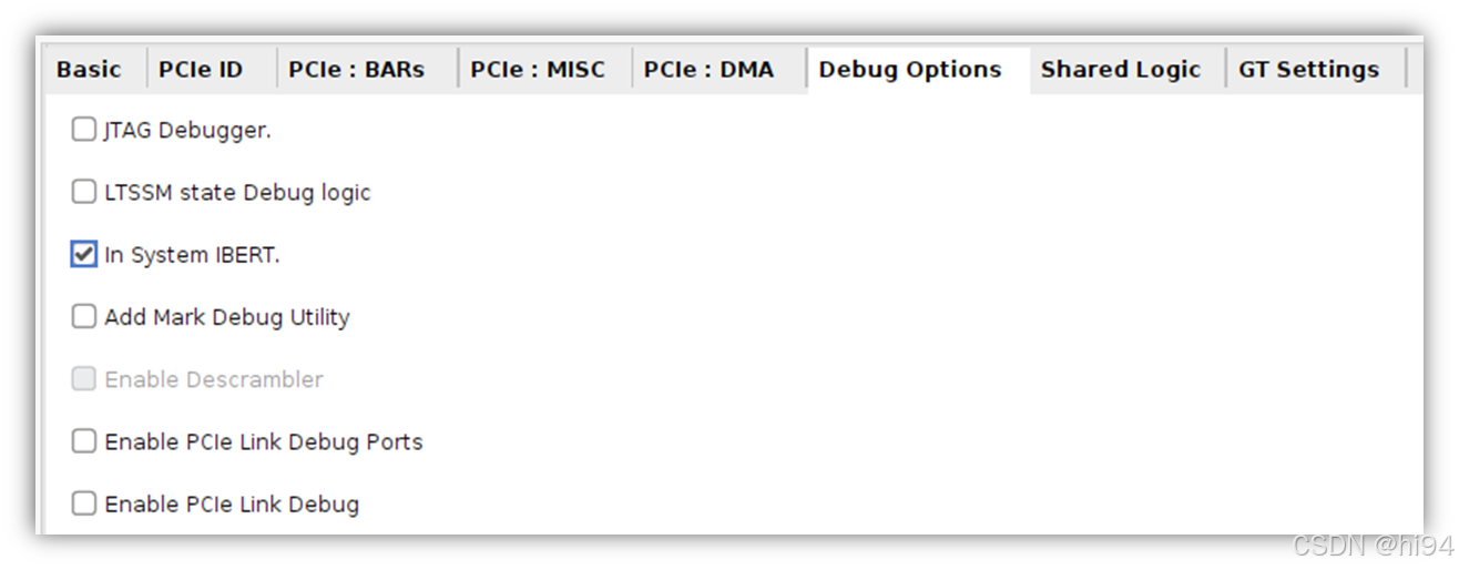
4.3.4 Debug Options
参考:《XAPP1198》
- In-system IBERT 可提供 PCIe 链接眼图。
- JTAG Debugger 和 In-system IBERT 功能结合在一起即可提供即时信息,用于判断链接训练错误的可能原因。
PCIe In-system IBERT 特点:
非侵入性检测:运行眼图扫描不影响链路完整性,保持信号裕量表征,结合收发器均衡器提供接收端信号裕量的最准确分析。
无需预设测试模式:PCI Express 链路很少使用环回模式,通常无预设测试模式,系统内眼图扫描可直接应用于运行中的链路。
容忍比特错误:即使存在比特错误,PCI Express 链路仍可保持在 L0 状态,通过 CRC 校验和重放机制确保数据完整性(但重放机制可能影响吞吐量)。
快速定位问题通道:多通道实现中,眼图扫描可快速识别信号裕量不足的具体通道,避免逐条排查的困难。
反映真实系统条件:扫描结果包含实际运行时依赖(如功耗、开关噪声等),覆盖空闲模式、DMA 模式等极端情况,无需人为启用测试模式。
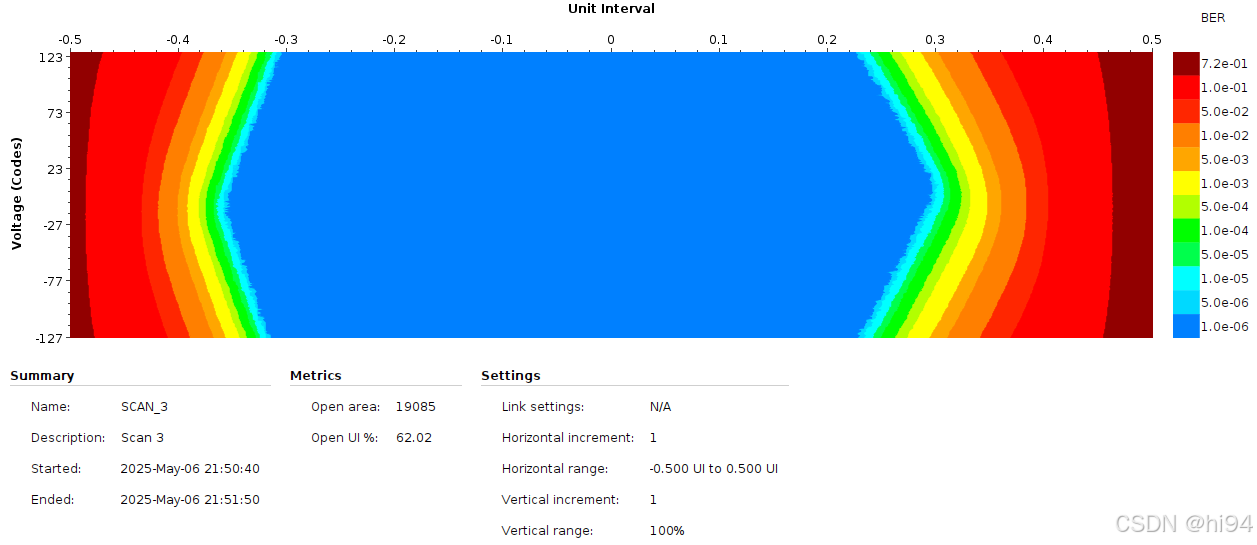
扫描条件:
4.3.5 信号完整性问题
1)通过延长线进行连接
>> sudo lspci -vv -s 01:00.0
---
01:00.0 Serial controller: Xilinx Corporation Device 9034 (prog-if 01 [16450])Subsystem: Xilinx Corporation Device 0007Control: I/O- Mem- BusMaster- SpecCycle- MemWINV- VGASnoop- ParErr- Stepping- SERR- FastB2B- DisINTx-Status: Cap+ 66MHz- UDF- FastB2B- ParErr- DEVSEL=fast >TAbort- <TAbort- <MAbort- >SERR- <PERR- INTx-Interrupt: pin A routed to IRQ 16Region 0: Memory at e1100000 (32-bit, non-prefetchable) [virtual] [size=1M]Region 1: Memory at e1200000 (32-bit, non-prefetchable) [virtual] [size=64K]
...LnkSta: Speed 8GT/s (ok), Width x4 (ok)
...Capabilities: [1c0 v1] Secondary PCI ExpressLnkCtl3: LnkEquIntrruptEn-, PerformEqu-LaneErrStat: LaneErr at lane: 0 2Kernel modules: xdma
要点:
- 可以识别 9034
- 重要功能无法使用,Control: Mem- BusMaster-
- PCIe Lane通道错误,LaneErrStat: LaneErr at lane: 0 2
- 可以看到 Kernel modules: xdma
2)直接连接 PCIe 板卡到主板
>> sudo lspci -vv -s 01:00.0
---
01:00.0 Serial controller: Xilinx Corporation Device 9034 (prog-if 01 [16450])Subsystem: Xilinx Corporation Device 0007Control: I/O- Mem+ BusMaster+ SpecCycle- MemWINV- VGASnoop- ParErr- Stepping- SERR- FastB2B- DisINTx-Status: Cap+ 66MHz- UDF- FastB2B- ParErr- DEVSEL=fast >TAbort- <TAbort- <MAbort- >SERR- <PERR- INTx-Latency: 0Interrupt: pin A routed to IRQ 141Region 0: Memory at e1100000 (32-bit, non-prefetchable) [size=1M]Region 1: Memory at e1200000 (32-bit, non-prefetchable) [size=64K]
...LnkSta: Speed 8GT/s (ok), Width x4 (ok)
..Capabilities: [1c0 v1] Secondary PCI ExpressLnkCtl3: LnkEquIntrruptEn-, PerformEqu-LaneErrStat: 0Kernel driver in use: xdmaKernel modules: xdma
要点:
- 可以识别 9034
- 功能正常识别,Control: Mem+ BusMaster+
- 可以看到 Kernel driver in use: xdma
5. 总结
本文详细介绍了基于 Xilinx ZCU102 开发板的 PCIe DMA 子系统设计与实现。
- DMA/Bridge Subsystem for PCIe 作为核心数据搬运引擎,通过描述符(Descriptor)实现主机内存与 FPGA 间的高效数据传输,支持连接不同AXI从设备(如 BRAM、DDR 或硬件加速器)。
- 在 ZCU102 平台上,Ubuntu 系统通过 PCIe 驱动(xdma.ko)管理设备,利用 lspci、setpci 等工具进行拓扑分析和寄存器配置。
- Vivado 工程中,XDMA IP 核的配置需注意 BAR 空间分配、时钟约束(如 IBUFDS_GTE 使用)及中断模式选择(轮询/中断)。
- 实际测试中,通过 reg_rw 和 dma_to_device 等工具验证了 H2C/C2H 通道传输功能,并针对信号完整性(如 PCIe 链路眼图扫描)和时序问题提供了调试方法。