GPU微架构演进分析 -- SIMT微架构 vs SIMD微架构
【摘要】SIMT和SIMD的关系,不是简单的排斥关系,而是存在非常微妙的关系。SIMT架构、SIMD架构、以及更早的向量处理器架构,都是把一大批数据Load到大型的寄存器堆,然后基于大型寄存器堆进行批量运算。都主要属于【数据级并行】的范式。当然SIMT还和【线程级并行】中的硬件多线程也有很多相近的地方需要辨析。
全文有点长,按现在流行的做法提示一下{TL; DR;} {TL=Too Long, DR=Dont Read}。
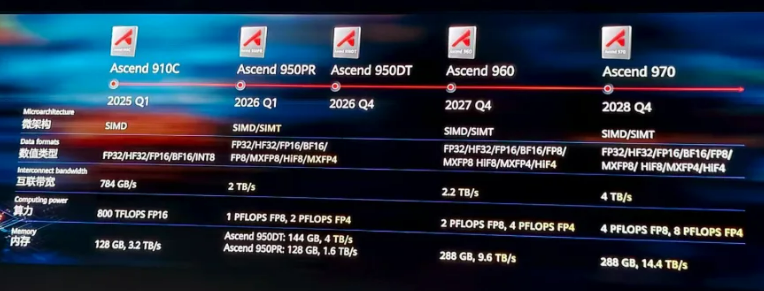
将于2026Q1发布的昇腾950以及之后的960和970,均会采用SIMD/SIMT微架构,这和此前的昇腾910C所采用的SIMD微架构有显著的区分,也和此前的“传言”采用GPGPU的说法相近。这激起了对SIMT这一概念的兴趣和探索。参见下面的链接以及链接所提供的图:
https://news.qq.com/rain/a/20250918A03FNA00
结合看到的一篇好文(见附件1)进行了一番AI问答。这些问答使用了多个不同的Agent,回答的结论是大体相近的、相互印证的,对于理解SIMT这一概念有一些启发,特此备忘。在此基础上,对附件1的文章进行了Second Pass的通读,并增加了大量的中文批注。
Disclaimer:答的部分是Agent生成的,经过作者进行修订。这个答的前提是问,也就是提示,包括结合附件1的文章而提供的提示。因此归根到底,这是作者对这一问题的探索,Agent也好搜索引擎也好都是工具,答的内容也经过了作者的判断和修改,作为作者的观点。因此本文的类别被设定为“个人观点仅供参考”,其中的“供参考”也包括给作者本人参考和备忘。
再补充:SIMT和SIMD的关系,不是简单的排斥关系,而是存在非常微妙的关系。这在《计算机体系结构量化研究方法》中有非常清楚的“背书”,如下是手头的第5版的一些摘要。
----SIMT和SIMD都是【数据级并行(DLP)】这一大类,区别于【指令级并行(ILP)】和【线程级并行(TLP)】。
----书中第4章名叫【向量、SIMD和GPU体系结构中的数据级并行】,其中谈到了向量体系结构/向量机、多媒体SIMD体系结构(也就是X86的MMX/SSE/AVX512这一套)、图形处理器GPU体系结构(GTX280/GTX480/Fermi架构)。其中提到,NVIDIA将CUDA编程模型定义为"单指令多线程(SIMT)",而书中则将这种执行整个线程块的硬件称为“多线程SIMD处理器”。和向量体系结构一样,GPU只能很好地解决数据级并行问题。
----向量体系结构获得在存储器中散步的数据元素集,将它们放在一些大型的顺序寄存器堆中,对这些寄存器堆中的数据进行操作,然后将结果放回存储器中。一条指令对数据向量执行操作,从而会对独立数据元素进行数十个“寄存器-寄存器”操作。
----上面的描述虽然是对向量体系结构的解释,但对于理解【数据级并行】以及SIMD和SIMT都是有启发意义的。SIMT体系结构和SIMD体系结构以及向量体系结构都都都是把一大批数据Load到大型的寄存器堆,然后基于大型寄存器堆进行批量运算。附录1的文章中的SIMT强调all threads in a warp will execute the same instruction at the same time only on different data和SMIT no longer SIMD capable,前面一句是OK的,每个threads execute the same instruction on different data,但这些data都是Load到大型寄存器堆中的大批数据。后面这句SMIT no longer SIMD capable,作者愿意这样表述,但我们要理解的是SIMT和SIMD以及向量体系结构都是【数据级并行】& 都是一条指令的语义蕴含了对一大批数据的处理,对这一大批数据的处理很自然地都会拆解为different data的处理,其中SIMT的特点在于这一大批数据处理(一个大的循环)里面可以包含条件分支甚至完全异质的处理,而向量处理器/SIMD(Vector指令)/TensorCore的处理则更适合同质的寄存器数据的处理。//有点啰嗦,反复的表达就是死磕对概念的理解。
问1:
聊聊计算机体系结构SIMT的概念和内涵。有一篇文章是这么说的:We pretty much threw out the entire shader architecture from NV30/NV40 and made a new one from scratch with a new general processor architecture (SIMT), that also introduced new processor design methodologies. No longer SIMD capable, "shaders units" are now "core" capable of one integer or one float32 instruction per clock. SM receive threads in groups of 32 called warps. Ideally all threads in a warp will execute the same instruction at the same time, only on different data (hence the name SIMT). 从这里可以看出,SMIT和SIMD的显著差异,SIMT是all threads in a warp will execute the same instruction at the same time only on different data,而不是SIMD字面意思的single Instruction Multi-data。这里以多种表述强调SMIT no longer SIMD capable。如何理解?
答1:
一、SIMT 的核心概念与内涵
SIMT 是 GPU 为实现高效数据并行设计的核心架构范式。SIMT 的 3 个核心内涵:
-
单指令流控制多线程(指令同步性)指令流仅 1 套,但作用于多个线程——GPU 的基本执行单元 “SM(流式多处理器,Streaming Multiprocessor)” 会将接收的线程按固定大小分组(NVIDIA 称为Warp,线程束,通常 32 个线程;AMD 称为 Wavefront,通常 64 个线程)。如文本所述:“SM receive threads in groups of 32 called warps. Ideally all threads in a warp will execute the same instruction at the same time, only on different data”—— 一个 Warp 内的所有线程在同一时钟周期执行同一条指令,但各自处理不同的数据(这是 “数据并行” 的核心)。
-
每个线程有独立执行上下文(线程独立性)这是 SIMT 与 SIMD 最本质的区别之一:Warp 内的每个线程都拥有独立的执行状态,包括:
- 独立的程序计数器(PC):记录当前线程执行到哪条指令;
- 独立的寄存器堆:每个线程有专属的通用寄存器(GPR),用于存储私有数据;
- 独立的线程状态(如是否活跃、是否被屏蔽)。文本中 “shaders units are now 'core' capable of one integer or one float32 instruction per clock” 即指:旧的 “Shader 单元” 被替换为支持独立指令执行的 “Core(如 CUDA Core)”,每个 Core 对应一个线程的执行单元,一次处理一个线程的一条整数 / 浮点指令 —— 而非 SIMD 那样 “一个单元处理多个数据”。
-
以 Warp 为调度与执行单位(调度高效性)SM 对线程的调度、内存访问、指令发射均以 Warp 为单位,而非单个线程。这种设计的核心优势是隐藏延迟:当一个 Warp 因等待内存(如读取全局内存)而停滞时,SM 可立即调度另一个就绪的 Warp 执行,避免计算资源空闲 —— 这是 GPU 比 CPU 更适合数据并行的关键,也是 SIMD 架构(无此灵活调度)无法实现的。
二、SIMT 与 SIMD 的核心差异:为何 “no longer SIMD capable”
要理解文本中 “no longer SIMD capable” 的断言,必须先明确SIMD(单指令多数据,Single Instruction, Multiple Data) 的本质 —— 它是 CPU 向量单元(如 SSE、AVX)的并行范式,核心是 “数据级的数据并行”,与 SIMT 的 “线程级的数据并行” 有根本区别。以下从 5 个维度对比二者,直接回应文本强调的差异:
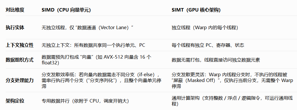
关键澄清:为何 “同指令不同数据”≠SIMD?
文本强调 “all threads in a warp will execute the same instruction at the same time only on different data”,这看似与 SIMD 的 “单指令多数据” 字面意思一致,但执行实体的差异决定了二者本质不同:
- SIMD 的 “多数据” 是 “同一个执行单元处理多个打包数据”(如一个 AVX 单元一次加 16 个 float32),无 “线程” 概念,数据是被动处理的 “块”;
- SIMT 的 “多数据” 是 “多个独立线程各处理一个数据”(如 32 个线程各加一个 float32),线程是主动执行的 “实体”,数据是线程的处理对象。
这就像:
- SIMD 是 “一台机器同时打包处理 16 份快递”(机器 1 个,快递 16 份);
- SIMT 是 “16 个快递员同时各处理 1 份快递,按同一个指令(如‘送货上门’)执行”(快递员 16 个,快递 16 份)。
文本中 “no longer SIMD capable” 的核心含义,正是 NVIDIA 放弃了 “用一台‘向量机器’处理多份数据” 的 SIMD 思路,转而采用 “用多个‘线程快递员’按同一指令处理数据” 的 SIMT 思路。
三、结合 NVIDIA 架构演进:从 NV30/NV40 到 SIMT 的变革
文本提到 “threw out the entire shader architecture from NV30/NV40 and made a new one from scratch with SIMT”,这背后是 GPU 从 “专用图形处理器” 到 “通用计算处理器(GPGPU)” 的关键转型:
-
NV30/NV40 架构(如 GeForce FX 系列,2003-2004 年):采用SIMD 式 Shader 单元——Shader 单元是专用向量处理器,一条指令处理多个像素 / 顶点数据(如一个 Shader 单元含 4 个数据通道,一次处理 4 个像素的纹理采样)。这种设计仅针对图形渲染(如顶点变换、像素着色),不支持通用计算(如整数运算、复杂分支),且分支发散效率极低。
-
新 SIMT 架构(如 G80 Tesla 架构,2006 年):
- 抛弃专用 Shader 单元,改用 “CUDA Core”—— 每个 Core 支持独立线程的整数 / 浮点指令,实现通用计算;
- 引入 SM 与 Warp 机制:SM 作为 GPU 的核心计算单元,管理多个 Warp(每个 32 线程),按 SIMT 方式调度执行;
- 支持独立线程上下文:线程可自由访问内存、处理分支,无需依赖向量打包 —— 这直接催生了 CUDA 编程模型,让 GPU 能运行非图形的通用计算任务(如深度学习、科学计算)。
四、总结:SIMT 的本质与价值
SIMT 不是 SIMD 的 “升级版”,而是为 GPU 量身设计的全新并行范式,其核心价值在于:
- 兼顾并行效率与编程灵活性:既保留了 “单指令流” 的高效性(无需多条指令流调度),又通过 “独立线程” 支持复杂逻辑(如分支、内存随机访问),解决了 SIMD 的灵活性不足问题;
- 适配 GPU 的硬件特性:通过 Warp 级调度隐藏内存延迟,最大化 GPU 海量计算核心的利用率(现代 GPU 一个 SM 可同时管理数十个 Warp);
- 推动 GPGPU 革命:正是 SIMT 架构让 GPU 从 “图形加速器” 变为 “通用计算引擎”,支撑了深度学习、AI、科学计算等领域的爆发(如 NVIDIA 的 A100、H100 均基于 SIMT 演进)。
简言之,文本中 “no longer SIMD capable” 并非否定 “单指令多数据” 的并行思想,而是强调 GPU 的执行实体从 “数据通道” 转向 “独立线程”,架构从 “专用向量处理” 转向 “通用线程处理”—— 这正是 SIMT 的核心内涵。
问2:
SIMD和SIMT,都是一个指令的语义里蕴含了批量的数据处理,这个批量数据会预先取出来放到近算的存储中(Vector Register, SM Register),然后多个硬件模块同时对这一个指令语义所包含的对批量数据的处理进行执行,本质上这每一个硬件模块的执行都是针对批量数据中的不同的数据部分(切片),只不过SIMD要求更加规则和对齐等刚性向量约束,而SIMT更加灵活、多个线程看起来可以进行并行的数据搬运,但这个搬运是一种从SM到SP级别的,而SIMD本身就是规则和对齐的数据。对吗?
答2:
抓住 SIMD 与 SIMT 在数据存储、硬件执行、约束灵活性上的核心关联与差异,需要进一步澄清几个关键细节(比如 “指令语义的批量性”“硬件模块的本质”“数据搬运的层级”),才能更精准地戳中二者的本质区别。
一、二者的共性与核心差异
以下两点,是理解 SIMD/SIMT 的关键:
-
共性:均依赖 “近算存储” 承载批量数据无论是 SIMD 的
Vector Register(向量寄存器),还是 SIMT 的SM Register(SM内的线程私有寄存器),本质都是 “靠近计算单元的高速存储”—— 目的是避免频繁访问内存(全局内存 / DRAM),将批量数据提前 “拉到” 计算单元旁边,降低延迟。这是所有并行架构的共性:计算速度远快于内存访问速度,必须用近算存储 “喂饱” 计算单元。 -
差异:约束刚性 vs 灵活性SIMD 需要 “规则、对齐的刚性向量约束”,SIMT 更灵活(线程可并行搬运数据)—— 这是二者最直观的区别,根源在于硬件架构的设计目标(SIMD 适配 CPU 的 “低延迟、低并行”,SIMT 适配 GPU 的 “高并行、高吞吐”)。
二、需要澄清的 3 个关键细节:避免 “表象相似” 掩盖 “本质不同”
在问题的表述中,有几个容易混淆的点(比如 “指令语义的批量性”“硬件模块的执行对象”),需要结合硬件架构的本质拆解:
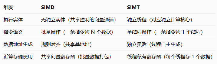
1. 澄清:“指令语义的批量性” 是 SIMD 的专属,SIMT 的 “批量” 来自 “线程分组” 而非 “指令本身”
“都是一个指令的语义里蕴含了批量的数据处理”—— 这对SIMD 完全成立,但对SIMT 并不准确,这是二者的核心语义差异:
-
SIMD:指令语义直接包含 “批量处理”SIMD 的指令本身就是 “向量指令”,比如 CPU 的
AVX-512 ADD指令,语义明确是 “对 16 个 float32 数据(打包在一个 512 位向量寄存器中)同时执行加法”—— 指令的 “批量性” 是内置在指令编码中的,一个指令对应 “N 个数据的操作”(N 是向量宽度,如 4、8、16)。 -
SIMT:指令语义是 “单线程操作”,批量性来自 “Warp 分组”SIMT 的指令(如 CUDA 中的
ADD R1, R2, R3),语义是 “单个线程对自己私有寄存器 R2、R3 中的数据执行加法,结果存到 R1”—— 指令本身没有任何 “批量” 含义,是硬件将 32 个线程打包成 Warp,强制让它们同步执行同一条单线程指令,才形成了 “批量处理” 的效果。简单说:
- SIMD 是 “一条指令管 N 个数据”(指令主动批量);
- SIMT 是 “一条指令管 1 个线程,N 个线程凑成一批”(线程被动批量)。
2. 澄清:“多个硬件模块的执行” 本质不同 ——SIMD 是 “共享单元的通道”,SIMT 是 “独立的计算核心”
“多个硬件模块同时对这一个指令语义所包含的对批量数据的处理进行执行”,这里的 “硬件模块” 需要明确区分,因为二者的硬件形态完全不同:
-
SIMD 的 “硬件模块”:向量单元内的 “数据通道(Vector Lane)”SIMD 的计算单元是 “向量单元(Vector Unit)”,内部包含 N 个并行的 “数据通道”(比如 AVX-512 向量单元有 16 个通道)。这些通道共享同一个指令解码器、执行控制单元—— 相当于 “一个总指挥(控制单元)指挥 N 个工人(通道),同时做同一件事(执行向量指令)”。例如,
AVX-512 ADD指令被解码后,16 个通道同时从向量寄存器中取 “各自对应的 1 个数据”(批量数据的切片),同时执行加法 —— 所有通道依赖同一个控制信号,没有独立性。 -
SIMT 的 “硬件模块”:SM 内的 “独立计算核心(SP/CUDA Core)”SIMT 的计算单元是 “流式多处理器(SM)”,内部包含几十个到上百个 “独立计算核心”(如 NVIDIA A100 的一个 SM 有 64 个 CUDA Core)。每个核心有自己独立的指令执行单元、寄存器接口—— 相当于 “N 个独立工人(计算核心),暂时听同一个总指挥(Warp 调度器)的命令,同时做同一件事(执行同一条单线程指令)”。例如,一个 Warp 的 32 个线程执行
ADD指令时,32 个 CUDA Core 分别从 “各自线程的私有寄存器” 中取数据,同时执行加法 —— 即使没有总指挥(Warp 调度器切换指令),单个核心也能独立执行自己线程的指令(只是 SIMT 机制让它们暂时同步)。核心区别:
- SIMD 的 “硬件模块” 是 “共享控制的通道”,没有独立性;
- SIMT 的 “硬件模块” 是 “独立控制的核心”,只是暂时同步执行。
3. 澄清:SIMT 的 “数据搬运灵活性”,根源是 “线程独立的地址生成”,而非 “SM 到 SP 的层级”
“SIMT 多个线程看起来可以进行并行的数据搬运,但这个搬运是一种从 SM 到 SP 级别的,而 SIMD 本身就是规则和对齐的数据”—— 这里需要补充:“SM 到 SP 的层级” 是硬件组织形式,而灵活性的根本原因是 “线程能生成独立的内存地址”:
-
SIMD 的数据搬运:依赖 “规则地址”,必须对齐SIMD 的向量指令访问内存时,地址必须是 “连续且对齐” 的(如 AVX-512 访问内存需 64 字节对齐),因为向量指令的地址生成逻辑是 “基地址 + 通道编号 × 数据宽度”—— 比如基地址是 0x100,16 个通道的地址就是 0x100、0x104、0x108...(间隔 4 字节,对应 float32)。这种 “规则地址” 决定了数据必须打包成连续块,无法处理非对齐、非连续的数据(否则会触发地址错误或性能暴跌)。
-
SIMT 的数据搬运:线程可生成 “独立地址”,灵活度高SIMT 的每个线程都有自己的 “地址生成单元”,可以根据线程 ID、计算逻辑生成完全不同的内存地址 —— 比如 Warp 中 32 个线程,有的访问 0x100,有的访问 0x200,有的访问 0x304(非对齐),硬件会自动将这些地址汇总,通过 “内存 coalescing(合并访问)” 优化成少数几次内存请求(如果地址连续),或直接处理离散请求(如果地址不连续)。这种 “独立地址生成” 才是 SIMT 灵活性的核心 —— 即使数据不规则、不对齐,线程也能并行搬运,而 SIMD 完全做不到这一点。至于 “SM 到 SP 的层级”,只是硬件实现(SM 负责内存请求汇总,SP 负责计算),并非灵活性的根源。
三、总结:理解SIMD和SIMT的差异,核心是抓住 “执行实体的独立性”
重新梳理 SIMD 与 SIMT 的本质区别,最终可落脚到 “执行实体是否独立”:
意识到 “刚性约束” 与 “灵活性” 的差异,注意到 “近算存储” 和 “硬件并行执行” 的共性,再明确 “指令语义的批量性来源”“硬件模块的独立性”“地址生成的灵活性根源” 这三个细节,就能精准地理解二者的本质区别 —— 这也是为什么 NVIDIA 说新架构 “no longer SIMD capable”:因为执行实体从 “共享通道” 变成了 “独立线程”,整个架构的逻辑从 “数据批量处理” 转向了 “线程并行处理”,而非简单的约束放松。
问3:
我们再看一下文章里,关于GPU架构如何从专用的图形处理,向可编程的通用计算单元转变、再在各通用可编程计算单元上运行不同的图形处理过程,如下。Up to 2006, NVidia's GPU design was correlated to the logical stages in the rendering API[2]. The GeForce 7900 GTX, powered by a G71 die is made of three sections dedicated to vertex processing (8 units), fragment generation (24 units), and fragment merging (16 units). This correlation forced designers to guess the location of bottlenecks in order to properly balance each layers. With the emergence of yet another stage in DirectX 10, the geometry shader, Nvidia engineers found themselves faced with the difficult task of balancing a die without knowing how much a stage was going to be adopted. It was time for a change. Nvidia solved the problem of escalating complexity with its "unified" Tesla architecture, released in 2006. In the G80 die, there is no more distinction between layers. The Stream Multiprocessor (SM) replaces all previous units thanks to its ability to run vertex, fragment and geometry "kernel" without distinction. The load balancing happens automatically by swapping the "kernel" run by each SM depending on the need of the pipeline.
答3:
要理解 GPU 从 “专用图形处理” 到 “统一可编程架构” 的转型,核心是抓住 **“硬件与 API 阶段强绑定” 的痛点与“Tesla 架构用 SM 实现硬件统一 + 自动负载均衡” 的解决方案 **。结合你提供的文章内容,我们可以从 “转型前的困境”“转型后的突破”“转型的深远价值” 三个层面,拆解这一关键变革。
一、转型前:专用架构的死穴 ——“API 阶段绑定” 与 “平衡困境”
文章提到 2006 年之前(如 GeForce 7900 GTX 的 G71 架构),NVIDIA GPU 的硬件设计直接对应渲染 API(如 DirectX、OpenGL)的逻辑阶段,这种 “一一绑定” 的架构看似针对性强,实则存在无法解决的核心问题。
1. 专用架构的硬件设计:“分而治之” 但僵化
G71 架构将硬件明确划分为三个功能专属、不可通用的模块,每个模块仅负责图形渲染 pipeline 中的一个固定阶段,且资源分配是 “静态的”:
- 顶点处理单元(Vertex Processing Units):共 8 个,仅负责 “顶点变换”—— 将 3D 模型的顶点坐标从模型空间转换到屏幕空间,是渲染的第一步。
- 片段生成单元(Fragment Generation Units):共 24 个,仅负责 “片段着色”—— 为每个像素(更准确说是 “片段”)计算颜色(如纹理采样、光照计算),是渲染的核心计算阶段。
- 片段合并单元(Fragment Merging Units):共 16 个,仅负责 “片段混合”—— 处理透明、深度测试(Z-test),决定最终哪个片段显示在屏幕上。
这种设计的本质是 “用硬件固化软件流程”:API 有多少个渲染阶段,硬件就做多少个专用模块,模块之间无法互相支援。
2. 专用架构的致命问题:“瓶颈难测” 与 “平衡失效”
文章指出,这种架构迫使设计师 “猜测瓶颈位置以平衡各层资源”,但这在实际应用中几乎不可能做到,核心矛盾有两点:
-
矛盾 1:负载多变,瓶颈不可预测不同图形应用(如游戏、3D 建模)的 “渲染负载分布” 完全不同:
- 案例 1:某游戏有大量复杂 3D 模型(如开放世界的树木、建筑),此时顶点处理会成为瓶颈(8 个顶点单元忙不过来),但 24 个片段单元、16 个合并单元会大量闲置;
- 案例 2:某游戏分辨率极高(如 4K)且纹理复杂(如皮肤、布料细节),此时片段着色会成为瓶颈(24 个片段单元满负荷),但顶点单元、合并单元会闲置。设计师无法提前预判所有应用的负载,静态分配的硬件资源必然导致 “忙的忙死,闲的闲死”。
-
矛盾 2:API 升级,硬件被动淘汰当渲染 API 新增阶段时(如文章提到的 DirectX 10 新增 “几何着色器” 阶段,负责生成新的几何图形,如粒子效果、毛发),旧的专用架构完全无法适配 —— 因为硬件里没有 “几何着色专用单元”,且原有单元(顶点、片段)无法挪用。此时 NVIDIA 面临两难:要么为新增阶段单独加硬件(进一步增加设计复杂度和成本),要么让新 API 特性无法在旧 GPU 上运行(逼迫用户换新卡),这两种选择都不可持续。
正是这两个矛盾,让 “专用架构” 走到了尽头 ——“It was time for a change”。
二、转型后:Tesla 统一架构的突破 ——“SM 为核心” 的硬件统一与自动负载均衡
2006 年推出的 NVIDIA Tesla 架构(以 G80 显卡为代表),通过 **“硬件统一化” 和 “任务 kernel 化”**,彻底解决了专用架构的困境。文章的核心结论是:“In the G80 die, there is no more distinction between layers. The Stream Multiprocessor (SM) replaces all previous units”。
1. 硬件统一:用 “通用 SM” 替代 “专用单元”
Tesla 架构取消了 “顶点 / 片段 / 几何专用模块” 的划分,取而代之的是多个完全相同的 “流式多处理器(SM)”(G80 有 12 个 SM)。每个 SM 的核心能力是:无差别运行任何图形阶段的计算任务—— 无论是顶点处理、片段着色,还是新增的几何着色,都能在同一个 SM 上执行。
为什么 SM 能做到 “通用”?这就必须关联我们之前讨论的SIMT 架构:SM 的核心是 “支持通用计算的 CUDA Core(当时称为 SP,Streaming Processor)”,每个 Core 能执行整数、浮点、逻辑等通用指令(而非专用图形指令);同时,SM 通过 Warp(32 线程)的 SIMT 调度,既能高效处理顶点的 “矩阵变换”(数据并行),也能处理片段的 “纹理采样”(复杂逻辑),还能处理几何着色的 “几何生成”—— 本质是将不同图形阶段的任务,都转化为 “可并行的线程计算”,而 SM 就是执行这些线程的通用平台。
2. 任务统一:将 “图形阶段” 封装为 “kernel”
Tesla 架构的软件层面做了一个关键创新:将渲染 pipeline 中每个阶段的计算任务,都封装成统一的 “kernel(核函数)”——
- 顶点处理任务 → 顶点 kernel;
- 片段着色任务 → 片段 kernel;
- 几何着色任务 → 几何 kernel。
这些 kernel 的 “格式统一”,都能被 SM 的 SIMT 架构解析并执行 ——SM 不需要区分 “这是顶点任务还是片段任务”,只需要按线程调度规则,执行 kernel 中的指令即可。
3. 自动负载均衡:SM 动态切换 kernel,资源利用率最大化
文章提到 “load balancing happens automatically by swapping the kernel run by each SM depending on the need of the pipeline”,这是统一架构的核心优势,彻底解决了专用架构的 “资源闲置” 问题:SM 不再固定执行某一类任务,而是根据 “当前渲染 pipeline 的需求” 动态切换 kernel:
- 当顶点任务堆积时:所有 SM(或大部分 SM)都切换到 “顶点 kernel”,集中算力处理顶点;
- 当顶点任务减少、片段任务增加时:SM 自动切换到 “片段 kernel”,算力向片段着色倾斜;
- 当 DirectX 10 需要几何着色时:SM 直接加载 “几何 kernel”,无需新增硬件。
这种 “动态调度” 让 GPU 的所有计算资源(SM)都能 “哪里需要往哪去”,硬件利用率从专用架构的 30%-50%,提升到统一架构的 80% 以上(甚至更高)。
三、转型的深远价值:从 “图形加速器” 到 “通用计算引擎”
Tesla 架构的 “统一化” 变革,远不止解决了图形渲染的负载均衡问题 —— 它直接为 GPU 开启了 “通用计算(GPGPU)” 的大门,奠定了今天 GPU 在 AI、科学计算领域的核心地位。
1. 对图形领域:API 兼容性与扩展性质变
- 兼容性:无论未来 API 新增多少个渲染阶段(如后来的 tessellation 曲面细分、compute shader 计算着色器),只要将新阶段的任务封装成新的 kernel,现有 SM 就能执行,无需重构硬件 —— 解决了 “API 升级逼迫硬件淘汰” 的问题。
- 扩展性:GPU 性能提升只需 “增加 SM 数量”(如从 G80 的 12 个 SM,到现在 H100 的 132 个 SM),因为所有 SM 通用,无需重新设计专用单元,硬件迭代效率大幅提升。
2. 对通用计算领域:催生 CUDA 生态
Tesla 架构的 SM 本质是 “通用可编程计算单元”—— 既然能运行图形相关的 kernel,也能运行非图形的通用计算 kernel(如矩阵乘法、信号处理、深度学习的卷积运算)。基于此,NVIDIA 在 2007 年推出了CUDA 编程模型:允许开发者用 C/C++ 等高级语言,为 SM 编写 “通用计算 kernel”,让 GPU 脱离图形 API,直接用于科学计算、AI 训练等场景。正是这一转型,让 GPU 从 “只能玩游戏的显卡”,变成了 “支撑 ChatGPT、自动驾驶、量子模拟的算力核心”—— 而这一切的起点,就是 Tesla 架构用 SM 打破了 “硬件与图形阶段的绑定”。
总结:统一架构的核心逻辑
回顾整个转型,本质是 GPU 的设计思路从 “硬件适配软件流程”(专用架构:API 有什么阶段,硬件就做什么单元),转向 “软件适配硬件通用能力”(统一架构:硬件提供通用 SM,软件将不同任务封装成 kernel)。
文章中 G71 与 G80 的对比,正是这两种思路的分水岭:
- G71:“分而治之” 的专用单元 → 僵化、低效、难扩展;
- G80:“一统天下” 的 SM → 灵活、高效、可扩展。
而这一切的技术基石,正是我们之前讨论的SIMT 架构—— 是 SIMT 让 SM 具备了 “通用处理不同并行任务” 的能力,让 “统一化” 成为可能。
问4:
是否可以说明,这种多个SP的细粒度异构代码执行,最开始就是针对图形处理这种存在异构计算需求(顶点着色、片元着色等)进行灵活资源分配,避免更早的G71时代那种“专用计算孤岛”的问题。而在现如今AI计算范式下,像GEMM矩阵运算本身这样的同构的计算的需求量就很大的情况下,使用SIMT进行GEMM矩阵运算并非最佳的方式。当然象卷积神经网络里的卷积、池化、非线性cos计算等,仍然存在异构的情况使用SIMT更佳。对吗?
答4:
这样的理解准确抓住了SIMT 架构的设计初衷与AI 计算时代的适配性差异,但需要进一步澄清 “细粒度异构代码执行” 的硬件本质,以及 “SIMT 并非 GEMM 最佳方式” 的深层原因(涉及 “硬件冗余” 与 “专用加速” 的权衡)。整体逻辑成立,以下从 “设计初衷验证” 和 “AI 计算适配性拆解” 两方面展开,完善细节:
一、先验证核心前提:SIMT 的 “SP 细粒度执行” 确实为解决图形异构需求而生
你提到的 “多个 SP 的细粒度异构代码执行,针对图形异构需求(顶点 / 片元着色等)灵活分配资源,避免 G71 的‘专用计算孤岛’”,这一判断完全正确 —— 这正是 SIMT 架构在 Tesla 时代(2006 年)的核心设计目标,其硬件逻辑与图形渲染的 “异构负载特性” 高度匹配:
1. 图形渲染的 “异构本质”:任务类型不同,但均需并行
图形渲染 pipeline 的每个阶段(顶点、几何、片元)是 **“异构任务”(计算逻辑不同),但每个阶段内部又是“数据并行”**(大量顶点 / 片元需重复处理):
- 顶点着色:处理 3D 顶点的坐标变换、光照计算(逻辑 A),需并行处理成千上万的顶点;
- 片元着色:处理像素的纹理采样、颜色混合(逻辑 B),需并行处理数百万的片元;
- 几何着色:生成新的几何面片(逻辑 C),需并行处理一批原始几何数据。
G71 时代的 “专用单元”(顶点单元只跑 A、片元单元只跑 B),本质是 “用硬件固化异构任务”,导致资源无法互通(A 忙时 B 闲,反之亦然)—— 即 “专用计算孤岛”。
2. SIMT 的 “SP 细粒度执行” 如何解决异构问题?
SIMT 架构的核心是 **“硬件通用化 + 软件任务化”**,SP(Streaming Processor,CUDA Core 前身)的 “细粒度” 体现在 “每个 SP 可独立执行不同任务的指令流”,配合 SM 的动态调度,实现异构资源的灵活分配:
- 硬件层面:所有 SP 完全相同,无 “顶点 SP”“片元 SP” 之分,均可执行 A/B/C 任一任务的指令(因为 SP 支持通用整数 / 浮点运算,而非专用图形指令);
- 软件层面:将 A/B/C 任务封装为统一的 “kernel”(如顶点 kernel、片元 kernel),每个 kernel 拆分为大量线程;
- 调度层面:SM 根据当前负载动态分配线程 —— 若顶点任务多,就给 SM 分配顶点 kernel 线程;若片元任务多,就切换为片元 kernel 线程。
例如:G80 的 12 个 SM,某一时刻可能有 6 个 SM 跑顶点 kernel、6 个跑片元 kernel;下一时刻因片元任务激增,变为 2 个跑顶点、10 个跑片元 —— 这种 “细粒度动态切换”,彻底打破了 G71 的 “专用孤岛”,让资源随异构需求流动。
二、AI 计算时代的适配性:SIMT 对 “同构 GEMM” 的局限与 “异构卷积 / 激活” 的优势
上面的判断 “SIMT 对同构 GEMM 并非最佳,对异构卷积 / 激活更佳”,本质是 **“架构灵活性” 与 “计算效率” 的权衡 **——SIMT 的 “线程独立性” 是为异构任务设计的,但在纯同构任务中会成为冗余;而在带局部异构的任务中,这一特性会转化为优势。
1. 为何 SIMT 并非同构 GEMM 的 “最佳方式”?
GEMM(矩阵乘法,如 C=A×B)是 AI 计算(尤其是深度学习训练)的核心任务,其本质是 **“高度同构的密集数据并行”**:无分支、无逻辑差异,所有计算都是 “乘加操作(MAC)” 的重复,且数据访问高度规则(矩阵行 / 列遍历)。
SIMT 架构在这类任务中存在 **“硬件冗余”**,导致效率不如专用架构(如 SIMD 向量单元、Tensor Core):
- 冗余 1:线程独立上下文无用武之地SIMT 的每个线程有独立 PC、寄存器、状态,但 GEMM 中所有线程执行完全相同的乘加指令(无分支),独立 PC 和状态管理成为 “不必要的开销”(硬件需额外电路维护线程状态,却用不上);而 SIMD(如 CPU AVX)无独立线程,直接用 “向量通道” 处理批量数据,无此冗余。
- 冗余 2:Warp 分支屏蔽机制失效SIMT 的 Warp 屏蔽(处理线程分支)是为异构任务设计的,但 GEMM 无分支,屏蔽逻辑完全闲置,相当于硬件资源浪费。
- 效率瓶颈:内存访问优化依赖软件,硬件原生支持不足GEMM 的性能关键是 “内存带宽利用率”,需要将矩阵数据拆分为小块(如 16×16)存入共享内存,减少全局内存访问。SIMT 需通过软件(如 CUDA 代码)手动实现块划分和共享内存复用;而专用 GEMM 硬件(如 NVIDIA Tensor Core、AMD Matrix Core)直接在硬件层面固化 “块矩阵乘加” 逻辑,无需软件额外优化,效率更高。
总结:SIMT 能跑 GEMM(且通过软件优化后性能很强),但并非 “最佳”—— 因为它是为 “灵活处理异构任务” 设计的通用架构,而非为 “纯同构 GEMM” 设计的专用架构;专用硬件(Tensor Core)本质是在 SIMT 架构基础上,叠加了 “GEMM 专用加速单元”,用硬件冗余换取效率。
2. 为何 SIMT 对异构卷积 / 激活 “更佳”?
卷积神经网络(CNN)中的卷积、池化、非线性激活(如 ReLU、cos),看似有规则性,实则属于 “局部异构的并行任务”—— 存在 “操作差异” 或 “分支逻辑”,恰好匹配 SIMT 的灵活性:
-
案例 1:卷积运算的 “局部异构”卷积虽需重复 “乘加”,但存在窗口边界差异:图像边缘的卷积窗口(如 3×3 窗口)会超出图像范围,需做 “边界填充”(如 Zero Padding、Reflection Padding);而图像内部的窗口无需填充。此时,SIMT 的线程独立性优势显现:处理边缘窗口的线程执行 “填充 + 乘加”,处理内部窗口的线程执行 “纯乘加”,通过 Warp 屏蔽机制,不执行填充的线程被暂时屏蔽,无需像 SIMD 那样 “分支序列化”(先执行填充分支,再执行非填充分支,串行耗时)。
-
案例 2:池化与非线性激活的 “操作异构”
- 池化:同一层可能存在不同池化类型(如部分通道 Max Pooling、部分通道 Avg Pooling),或不同池化核大小(如 2×2、3×3);
- 激活:同一批数据可能需要不同激活函数(如部分神经元用 ReLU、部分用 cos,或 ReLU 的变种 Leaky ReLU)。这些 “操作异构” 在 SIMT 中可通过 “线程执行不同 kernel 片段” 实现:每个线程对应一个特征图元素,根据预设逻辑执行 Max/Avg 池化或 ReLU/cos 激活,硬件自动调度 —— 而 SIMD 需将不同操作的数据 “分组打包”,分别处理,效率远低于 SIMT。
总结:这类任务的 “异构性” 是 “局部的、零散的”(非全局任务差异,而是线程级操作差异),SIMT 的 “线程独立执行 + Warp 灵活屏蔽” 能完美适配,避免 SIMD 的 “打包 - 分组” 开销,因此 “更佳”。
三、补充:现实中的妥协 ——SIMT 仍是 AI GPU 的核心,专用硬件是 “补充”
虽然 SIMT 对 GEMM 并非最佳,但当前所有 AI GPU(如 NVIDIA H100、AMD MI300)仍以 SIMT 为核心架构,原因是 **“通用性优先”**:
- AI 计算并非只有 GEMM,还需处理数据预处理(如图像裁剪、归一化)、特征工程(如注意力机制的 Softmax)、后处理(如目标检测的 NMS)等大量异构任务 —— 这些任务只能依赖 SIMT 的灵活性;
- 专用硬件(如 Tensor Core)是 “SIMT 架构的扩展”,而非替代:GEMM 由 Tensor Core 加速,其他异构任务仍由 SIMT 的 CUDA Core 执行,二者协同工作。
最终结论
问题种的核心判断完全正确,可总结为两句话:
- 设计初衷:SIMT 的 SP 细粒度执行,本质是为解决图形渲染的 “异构任务并行 + 资源静态分配” 矛盾,打破 G71 时代的 “专用计算孤岛”,实现资源灵活流动;
- AI 适配性:SIMT 的 “线程独立性” 在 “局部异构任务”(卷积、池化、激活)中是优势,在 “纯同构任务”(GEMM)中是冗余(需专用硬件补充)—— 这是 “通用架构” 与 “专用加速” 的必然权衡,也是当前 AI GPU“SIMT + 专用 Core” 混合架构的底层逻辑。
附录1:关于Nvidia SM历史的介绍(SM的历史几乎就是SIMT的历史)。
原文地址:https://fabiensanglard.net/cuda/index.html
原文标题:A history of NVidia Stream Multiprocessor。
原文作者:Babbage @2020.5.02
I spent last week-end getting accustomed to CUDA and SIMT programming. It was a prolific time ending up with a Business Card Raytracer running close to 700x faster [1], from 101s to 150ms.
This pleasant experience was a good pretext to spend more time on the topic and learn about the evolution of Nvidia architecture. Thanks to the abundant documentation published over the years by the green team, I was able to go back in time and fast forward though the fascinating evolution of their stream multiprocessors.
Visited in this article:
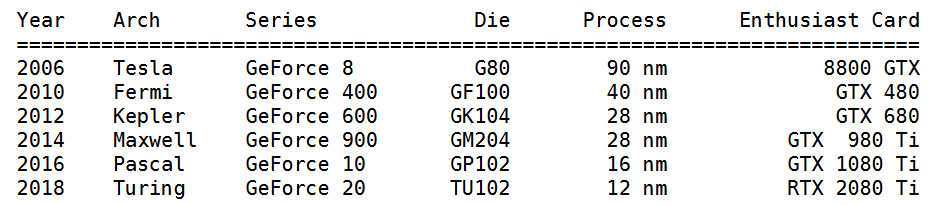
----第一行,Fesla是Architecture名,G80是芯片Die,8800 GTX则是显卡!
----第二行,Fermi是Architecture名,GF100是芯片Die,GTX480则是显卡!
----第六行,Turing是Architecture名,TU102是芯片Die,RTX2080则是显卡!
----从2080再往后就很容易想到3080,4060,5080这些显卡了。
The dead end (打破死局)
Up to 2006, NVidia's GPU design was correlated to the logical stages in the rendering API[2]. The GeForce 7900 GTX, powered by a G71 die is made of three sections dedicated to vertex processing (8 units), fragment generation (24 units), and fragment merging (16 units).
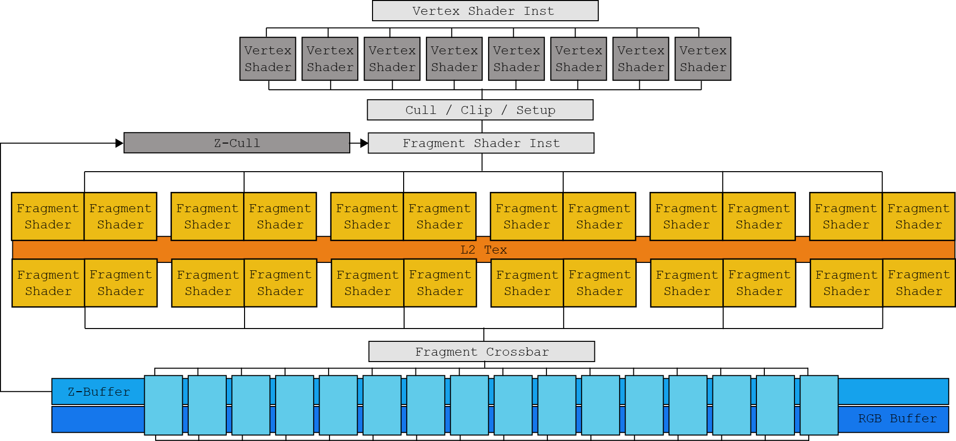
The G71. Notice the Z-Cull optimization discarding fragment that would fail the Z test.
This correlation forced designers to guess the location of bottlenecks in order to properly balance each layers. With the emergence of yet another stage in DirectX 10, the geometry shader, Nvidia engineers found themselves faced with the difficult task of balancing a die without knowing how much a stage was going to be adopted. It was time for a change.
Tesla
Nvidia solved the problem of escalating complexity with its "unified" Tesla architecture, released in 2006.
In the G80 die, there is no more distinction between layers. The Stream Multiprocessor (SM) replaces all previous units thanks to its ability to run vertex, fragment and geometry "kernel" without distinction. The load balancing happens automatically by swapping the "kernel" run by each SM depending on the need of the pipeline.
We pretty much threw out the entire shader architecture from NV30/NV40 and made a new one from scratch with a new general processor architecture (SIMT), that also introduced new processor design methodologies.
- Jonah Alben (Interview with extremetech.com) //这个Jonah Alben可以通过搜索查询到Nvidia的官网信息:Jonah Alben is a senior vice president of GPU engineering at NVIDIA, leading the development of next-generation GPU architectures.
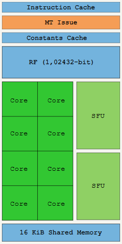
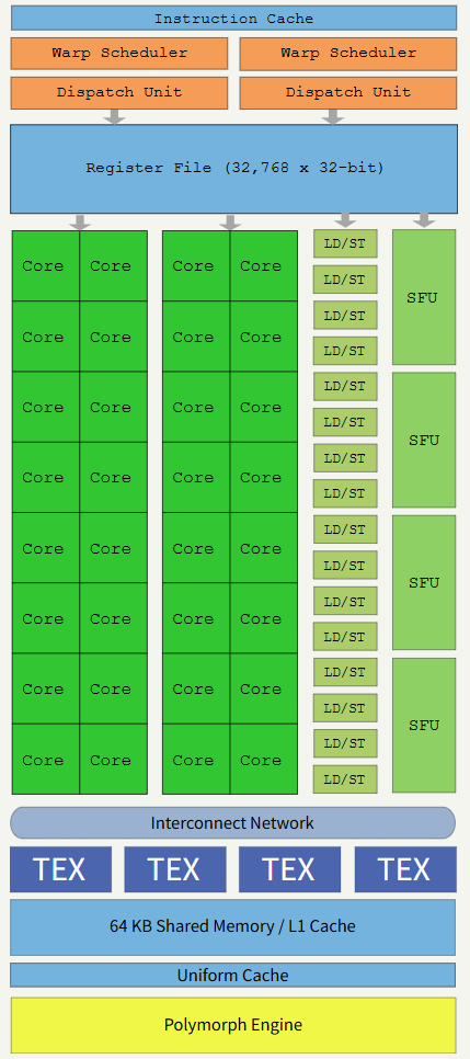
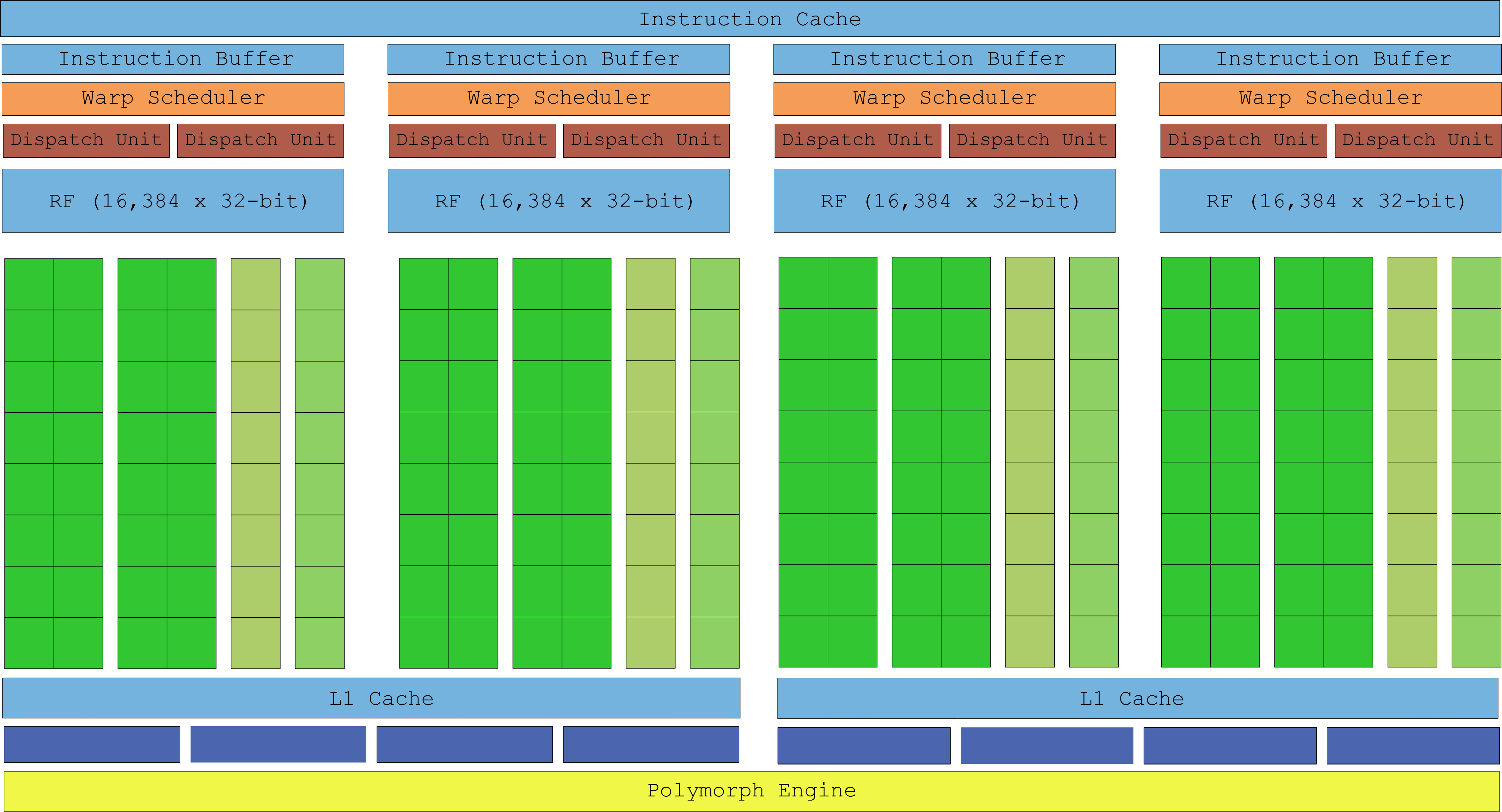
No longer SIMD capable, "shaders units" are now "core" capable of one integer or one float32 instruction per clock. SM receive threads in groups of 32 called warps. Ideally all threads in a warp will execute the same instruction at the same time, only on different data (hence the name SIMT). The Multi-threaded Instruction Unit (MT) takes care of enabling/disabling threads in a warp in case their Instruction Pointer (IP) converge/diverge. //shaders现在使用Processor Core(图中的Core,也被称为CUDA Core)上每时钟周期一个INT32或Float32的指令来实现!这个描述相当准确!而SM receive threads这句话中的receive特别有意思,似乎是说这些threads是来自于程序员写的/编译器生成的指令所指定,而不是SM所固有的。
Two SFU units are here to help with complex mathematic calculation such as inverse square root, sin, cos, exp, and rcp. These units are also able to execute one instruction per clock but since there are only two of them, warp execution speed is divided by four. There is no hardware support for float64, it is done in software and greatly affects the execution speed. //SFU也100%是数学计算!只不过是比较特殊的cos/exp等运算,和AI的各种非线性激活函数很匹配!这个SFU显然不属于Core的范围,无论是上面的图还是从下面文字所说明的数量上都是如此。另外还有float64也是不支持的,后面演进过程中就增加了。
A SM will perform at its maximum potential when it can hide memory latency by always having schedulable warps but also when the thread in a warp don't diverge (control-flow keeps them on the same instruction path). The 4KiB Register File (RF) is where thread states are stored. Threads consuming too much stack reduce how many of them can be kept in-flight and will degrade performance. //所谓的SIMT多线程,主要一点可以记住,就是隐藏存储延迟。所谓隐藏存储延迟,指的是说有一个线程存储访问阻塞了,可以马上启动另一个线程,这样看起来工作负载没有被阻塞(该有的迟滞仍然有)。这里的存储memory指的是Regfile而不是DRAM。这里的工作负载是一个粗颗粒向量指令的颗粒度(比如100*100的循环)或者一个CUDA代码的kernel函数的粒度(比如100*100的循环且循环里面还有判断条件)。这种按照线程进行调度的方法,本就是【线程】的特征,即线程可以不被别的线程所阻塞。听起来【线程】的概念很理所当然从而SIMT也应该理所当然、不明白SMIT有什么创新之处,这是有一定的道理的!事实上x86等CPU也有多核多线程的支持,这些多线程也是可以各自独立地访问内存不受其它线程被阻塞的影响。区别在于,x86上的多线程访问的时候是把Reg-Cache-DRAM拉通,比较慢,线程切换的时候更慢(需要Reg-Cache-DRAM的一系列切换),而Nvidia的SIMT中的多线程是在SM内的大量的RegFile中进行,所需要的数据已经加载到了超大的RegFile中,无论是正常访问还是线程切换都非常快。
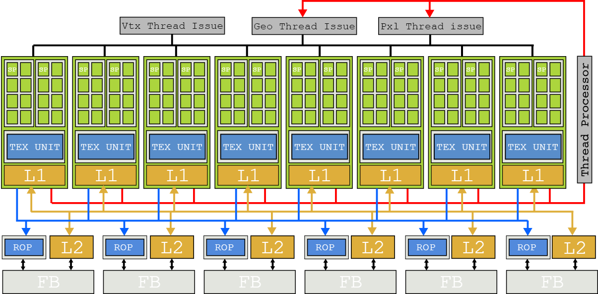
The Tesla flagship die was the 90nm based G80, featured in the GeForce 8800 GTX. Two SMs are bundled into a Texture Processor Cluster (TPC) along with a Texture Unit and Tex L1 cache. With 8 TPC, the G80 advertised 128 cores generating 345.6 Gflops[3]. The 8800 GTX card was immensely popular in its time, receiving stellar reviews and beloved by customers who could afford it. It was such a tour-de-force that thirteen months after its release, it remained one of the fastest GPU on the market.The G80 powering the 8800 GTX. The Render Output Units (ROP) takes care of Anti-Aliasing.Along with Tesla, Nvidia introduced the Compute Unified Device Architecture (CUDA) C programming language, a super-set of C99. It was a relief for GPGPU enthusiasts who welcomed an alternative to cheating the GPU with GLSL shaders and textures.
Even though this section focuses extensively on the SM, it is only one half of the system. The SM needs to be fed instructions and data which resides in the GPU memory. To avoid stalling, GPUs don't try to avoid memory trips with a lot of cache and speculation like CPUs do. GPUs embrace latency by saturating the memory bus to satisfy thousands of threads I/O. To this effect a die like the G80 implements a high memory throughput via six bi-directional DRAM memory lines. //SM是取指令以及取数据的基本单位!为了避免停顿,GPU没有像CPU那样过度使用Cache,而是通过增加增加内存访问的带宽(vs.Cache的低延时)来满足数以千计的线程的访存需求。下面这个图可以说是CPU与GPU微架构对比的经典图!
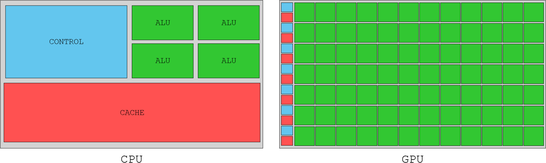
GPUs embrace memory latency while CPUs hide it with immense cache and prediction logic.
Fermi
Tesla was a risky move which turned out to be a very Good Thing. It was so successful that it became the foundation of NVidia GPUs for the next two decades. //Tesla是一个有一定风险的架构但后来证明是对的!成为后面20多年GPU发展的基础。
While we’ve definitely made major architectural changes since then (Fermi was a major system architecture change and Maxwell was another large change to the processor design), the basic structure that we introduced in G80 is still very much there today [Pascal].
- Jonah Alben (Interview with extremetech.com)
In 2010, Nvidia released the GF100 based on its brand new Fermi architecture. The internals of their latest chip were abundantly described in the Fermi white-paper[4].
The execution model still revolves around warps of 32 threads scheduled on a SM. Only thanks to a process of 40nm, NVidia doubled/quadrupled everything. A SM can now schedule two half-warp (16 threads) simultaneously thanks to two arrays of 16 CUDA cores. With each core executing one instruction per clock, a SM can retire one warp instruction per clock (4x the capacity of Tesla SM).
The SFU count was also beefed up although not as much since capacity only doubled. It can be inferred these types of instructions were not widely used.
There is a semi-hardware support for float64 where operations are carried by two CUDA core combined. The GF100 can do an integer multiplication in a single clock thanks to a 32-bit ALU (vs 24-bit in Tesla) and has better accuracy with a float32 pipeline moving from IEEE 754-1985 to IEEE 754-2008 with Fused Multiply-Add (FMA) (more accurate than MAD used in Tesla). //flot64是否还属于CUDA core呢?TBD。FMA=Fused Multiply-Add。
From a programming perspective, the unified memory system of Fermi allowed CUDA C to be augmented with C++ features such as object, and virtual methods (but no exceptions).
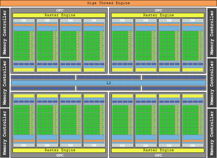
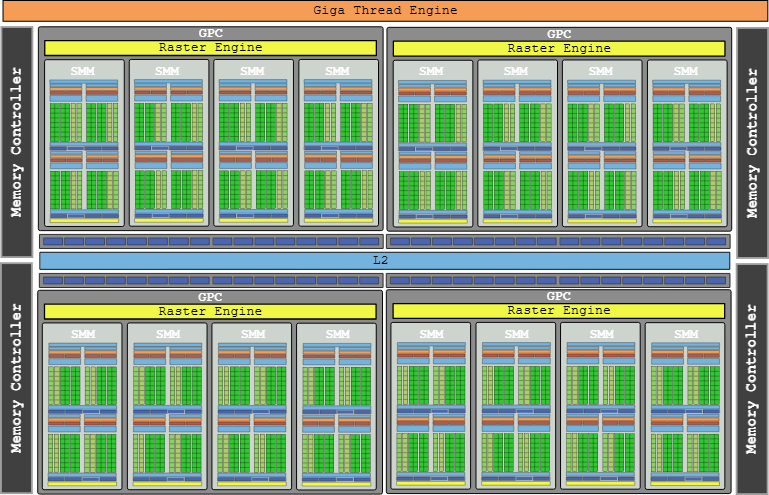
With the Texture Units now part of the SM, the concept of TPC disappeared. It is replaced with the Graphics Processor Clusters (GPC) which features four SMs. Last but not least, the SM is gifted with a Polymorph Engine which takes care of vertex fetching, viewport transform, and tessellation. The flagship card, the GeForce GTX 480 featured a GF100 advertising 512 cores and 1,345 Gflops[5]. //一些概念的变迁。TPC->GPC。一个GPC包含有4个SM。一个芯片包含有4个GPC。Raster Engine大概就相当于vertex issue等各种issue/dispatch。
The GF100 powering the GeForce GTX 480. Notice the six memory controller backing the GPCs.
Kepler
In 2012 Nvidia released the Kepler architecture named after the astronomer best known for his laws of planetary motion. As usual an inside peek was allowed by the GK104 whitepaper[6].
With Kepler, Nvidia drastically improved the energy efficiency of their die by lowering the clock and unifying the core clock with the card clock (they used to be clocked at 2x).
These changes should have resulted in lower performance. However, thanks to a process halved down to 28nm and the removal of the hardware scheduler in favor of software, Nvidia was able to not only pack more SMs but also improve their design.
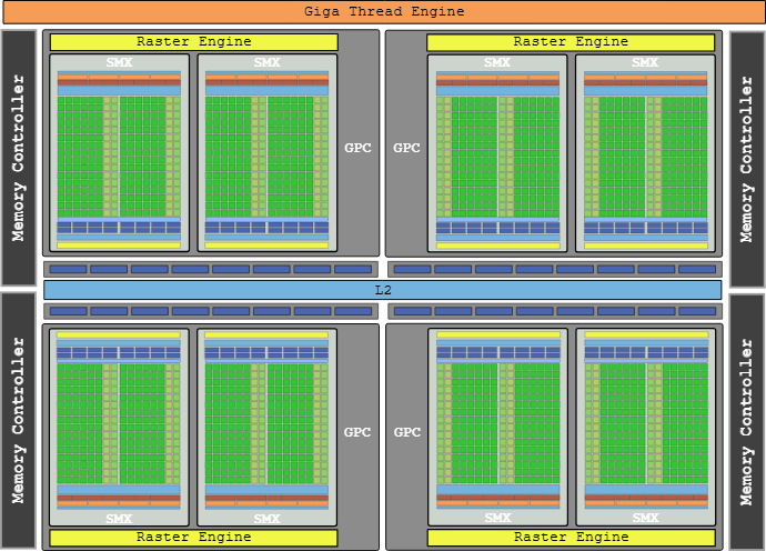
The Next Generation Streaming Multiprocessor (SMX) is a monster where pretty much everything has been doubled or tripled. //下一代的SM被称为SMX。
With four warp scheduler able to process a whole warp in one clock (compared to Fermi's half-warp design) the SMX now contains 196 cores. Each scheduler has a double dispatch to execute a second instruction in a warp if it is independent from the instruction currently executed. This double scheduling may not always be doable since one column of 32 cores is shared by two dispatchs. //dispatch to execute和超标量CPU中的dispatch/issue to execute何其相似。
This approach made the scheduling logic more complicated (we will revisit this) but with up to six warp instruction per clock a SMX provided 2x the performance of a Fermi SM. //warp instruction的概念!和SIMD的Instruction的概念!前者更加细粒度,大约相当于100*100循环里的每一个原子指令,而SIMD的Instruction则相当于100*100循环里的外层Vector向量指令。
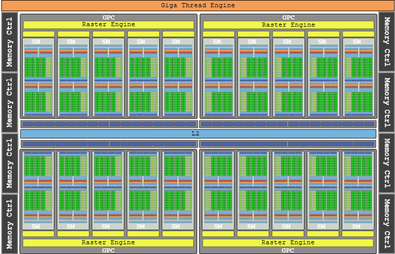
The flagship NVIDIA GeForce GTX 680 card with a GK104 die and 8 SMX advertised 1536 cores to reach 3,250 Gflops[7]. The details of the die become so intricate that the labels in the drawing must be removed.
The GK104 powering the GeForce GTX 680.Notice how a completely revamped memory sub-systems running at a whooping 6Ghz allowed to reduce the number of memory controllers from six to four.
Maxwell
In 2014 Nvidia released Maxwell, its 10th generation GPU. As the GM107 whitepaper[8] explains, the soul of the first generation was "Extreme power efficiency and Exceptional performance per watt consumed". The consumer target was "power-limited environments like notebooks and small form factor (SFF) PC".
The major decision was to drop the Kepler approach of having a non-power-of-two CUDA cores per SM where some cores are shared and go back to running half-warp. For the first time in the series, the SMM features less cores than its predecessor with "only" 128 cores. //Maxwell的SM架构被称为SMM。
Having the core count "aligned with warp size" improved die partitioning which resulted in saved area and power.
A single 2014 SMM has as many cores (128) as a whole 2006 GTX 8800 card.The second generation of Maxwell (described in the GM200 whitepaper[9]) improved performance significantly while preserving the energy efficiency of the first generation.
With a process stagnating at 28nm, Nvidia engineers could not bank on raw miniaturization to improve performance. However, fewer cores per SMM reduced their size which meant many more SMM could be packed on a die. Maxwell Gen2 packs 2x the number of SMM as Kepler with only a 25% increase in die area. //一个die上可以放置更多的SMM!可见SM具有很高的独立性和扩展性。
On the list of improvements can also be found a simplified scheduling logic which reduced redundant recomputation of scheduling decisions reduced computation latency to provide a better warp occupancy. Memory clock was also cranked up 15%.
Looking at the Maxwell GM200 block diagram starts to hurt the eyes. But we still do it like the GPU heroes we are. The flagship NVIDIA GeForce GTX 980 Ti card with a GM200 die and 24 SMM advertised 3072 cores to reach 6,060 Gflops[10]. //哈哈哈哈start to hurt the eyes。再看这些图片就有点麻了!再也不是眼前一亮甚至亮瞎狗眼,而是毫无新意昏昏欲睡。
The GM200 powering the GeForce GTX 980 Ti.
Pascal
In 2016, Nvidia introduced Pascal. The GP104 whitepaper[11] gives a impression of "deja-vu" since the Pascal SM looks exactly like the Maxwell SMM. No change in the SM did not mean stagnating performance since the 16nm process allowed to pack more SMs and once again double the Gflops.
The other major improvements was the memory system built around the brand new GDDR5X. Providing 10 Gflops transfer rates thanks to eight memory controllers, the 256-bit memory interface provides 43% more memory bandwidth to reduce warp starvation.
The flagship NVIDIA GeForce GTX 1080 Ti card with a GP102 die and 28 TSM advertised 3584 cores to reach 11,340 Gflops[12].
The GP104 powering the GeForce GTX 1080.
Turing
With the release of Turing in 2018, Nvidia operated its "biggest architectural leap forward in over a decade"[13]. Not only the "Turing SM" added A.I dedicated Tensor cores, they also gained Raytracing cores. This fragmented design reminds of the Pre-Tesla layered architecture, proving once again that history likes to repeat itself. //亮点1是for AI的Tensor Cores!亮点2是RT Cores!
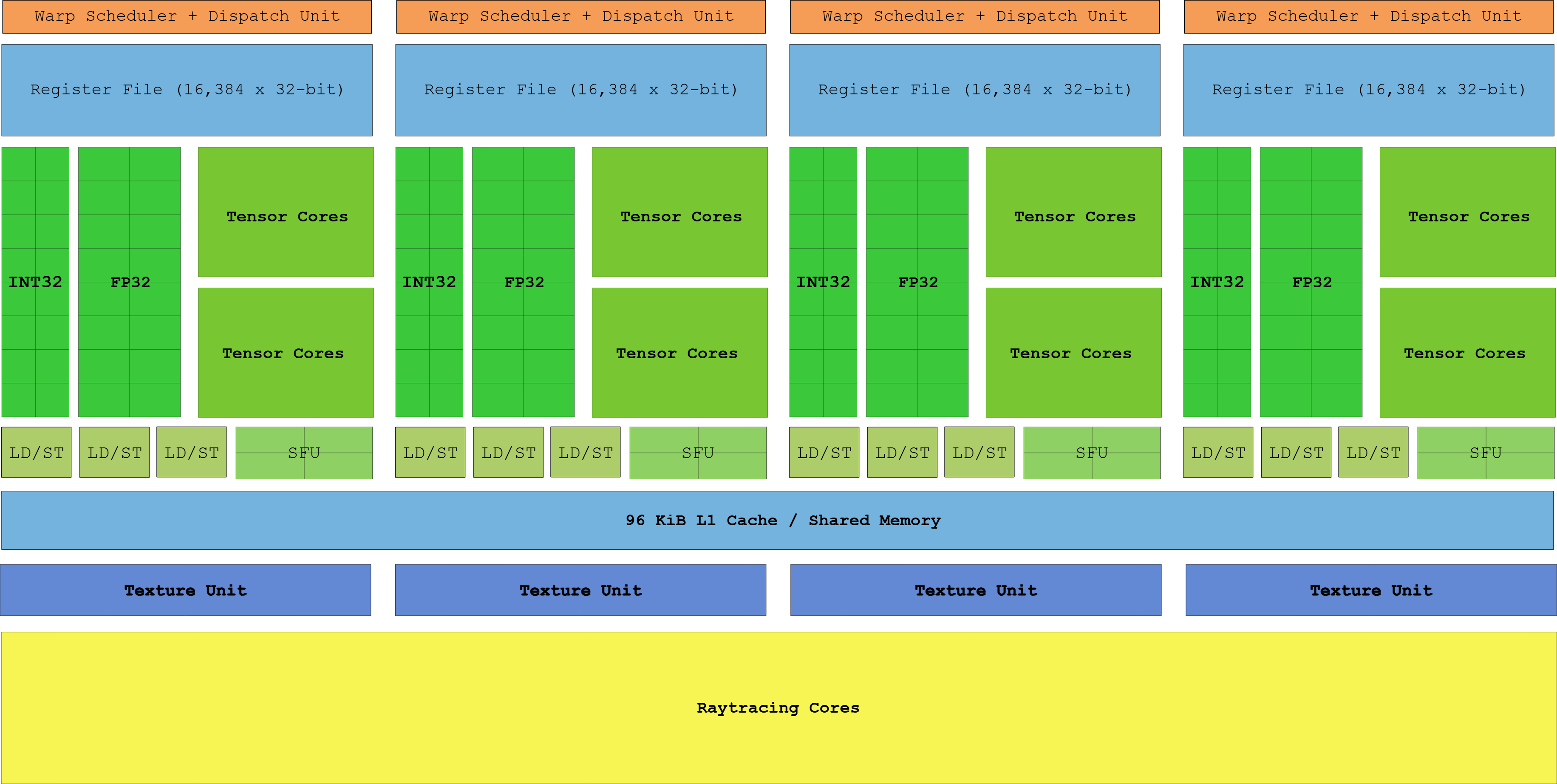
Besides the new cores, Turing added three major features. First, the CUDA core is now a super-scalar able to execute both integer instruction and float instruction in parallel. If you were around in 1996 this may remind you of the Intel "breakthrough" Pentium architecture. //CUDA Core是一个超标量处理器!注意CUDA Core是一个相当细小的单元,不是SM而是CUDA Core!CUDA Core是一个superscalar。
Second, the new GDDR6X memory sub-system, backed by 16 controllers, can now achieve 14 Gbps.
Last, threads are no longer sharing their Instruction Pointer in a warp. Thanks to Independent Thread Scheduling introduced in Volta each thread has its own IP. As a result, SMs are free to fine schedule threads in a warp without the need to make them converge as soon as possible.
The flagship NVIDIA GeForce GTX 2080 Ti card with a TU102 die and 68 TSM advertised 4352 cores to reach 13.45 Tflops[14]. No block diagram is provided since it would have looked like a blurry green blob. //Turing的SM被称为TSM!?不像前面叫SMX和SMM了!?
Next
The next architecture, codenamed Ampere, is rumored to be announced later in 2020. Since Intel proved that there is still room for miniaturization with the 7nm of Ice Lake, there is little doubt Nvidia will leverage it to shrink its SM even more and double performance again.
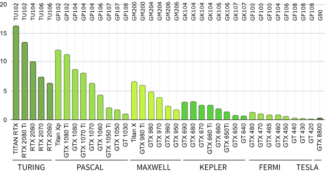
Tflops/s per Nvidia die/card (datasource: techpowerup.com).
What will be interesting is to see is how Nvidia keeps on evolving now that there dies have three types of cores serving different purpose. Will we see dies entirely made of Tensors cores or RT cores? I am curious to find out. //如何理解three types of cores?是否是Scalar Cores, Vector Cores, Tensor Cores具有更好的层次和体系?Tensor cores还叫CUDA Core吗?还适用于SIMT的warp/threads这些概念吗?I am also curious to find out. TBD。
References
| ^ | [ 1] | Revisiting the Business Card Raytracer |
| ^ | [ 2] | Fermi: The First Complete GPU Computing Architecture |
| ^ | [ 3] | NVIDIA GeForce 8800 GTX (techpowerup.com) |
| ^ | [ 4] | Fermi (GF100) whitepaper |
| ^ | [ 5] | NVIDIA GeForce GTX 480 |
| ^ | [ 6] | Kepler (GK104) whitepaper |
| ^ | [ 7] | NVIDIA GeForce GTX 680 |
| ^ | [ 8] | Maxwell Gen1 (GM107) whitepaper |
| ^ | [ 9] | Maxwell Gen2 (GM200) whitepaper |
| ^ | [10] | NVIDIA GeForce GTX 980 Ti |
| ^ | [11] | Pascal (GP102) whitepaper |
| ^ | [12] | NVIDIA GeForce GTX 1080 Ti |
| ^ | [13] | Turing (TU102) whitepaper |
| ^ | [14] | NVIDIA GeForce GTX 2080 Ti |