高通Camera点亮3——Camera Module
Camera点亮除了Sensor之外还需要配置module、EEPROM等,multicamera;配置好编译设置。
Module
<?xml version="1.0" encoding="utf-8" ?>
<cameraModuleData
    <!--Module group can contain either 1 module or 2 modules
      Dual camera, stereo camera use cases contain 2 modules in the group -->
  <moduleGroup>
    <!--Module configuration -->
    <moduleConfiguration description="Module configuration">
      <!--CameraId is the id to which DTSI node is mapped.
          Typically CameraId is the slot Id for non combo mode. -->
      <!--cameraId字段与Camera设备树中的配置的id需要保持一致,同时multicamera中的soltId也对应该值-->
      <cameraId>6</cameraId>
      <!--Name of the module integrator -->
      <moduleName>united</moduleName>
      <!--Name of the sensor in the image sensor module -->
      <!--对应的Sensor名,与Sensor XML中定义需要一样-->
      <sensorName>ov13b10</sensorName>
      <!--Actuator name in the image sensor module
          This is an optional element. Skip this element if actuator is not present -->
      <!--马达名称,与文件中的定义需要对应一致-->
    <actuatorName>dw9714v</actuatorName>
    <!-- Element for actuatorSlaveAddress -->
    <actuatorSlaveAddress>0x18</actuatorSlaveAddress>
      <eepromName>p24c64e</eepromName>
      <flashName>pmic</flashName>
      <!--Chromatix name is used to used to open binary.
          Binary name is of the form sensor_model_chromatix.bin -->
      <chromatixName>united_ov13b10</chromatixName>
      <!--Position of the sensor module.
          Valid values are: REAR, FRONT, REAR_AUX, FRONT_AUX, EXTERNAL -->
      <position>REAR</position>
      <!--CSI Information -->
      <CSIInfo description="CSI Information">
          <!--MIPI数据lane的分布-->
          <laneAssign>0x3210</laneAssign>
          <isComboMode>0</isComboMode>
      </CSIInfo>
      <!--Lens information -->
      <lensInfo description="Lens Information">
        <!--Focal length of the lens in millimeters. -->
        <focalLength>3.34</focalLength>
        <!--F-Number of the optical system. -->
        <fNumber>2.2</fNumber>
        <!--Minimum focus distance in meters. -->
        <minFocusDistance>0.1</minFocusDistance>
        <!--Total focus distance in meters. -->
        <maxFocusDistance>8.0</maxFocusDistance>
        <!--Horizontal view angle in degrees. -->
        <horizontalViewAngle>68.4</horizontalViewAngle>
        <!--Vertical view angle in degrees. -->
        <verticalViewAngle>53</verticalViewAngle>
        <!--Maximum Roll Degree. Valid values are: 0 to 359 -->
        <maxRollDegree>360</maxRollDegree>
        <!--Maximum Pitch Degree. Valid values are: 0, 90, 180, 270 -->
        <maxPitchDegree>360</maxPitchDegree>
        <!--Maximum Yaw Degree. Valid values are: 0 to 359 -->
        <maxYawDegree>360</maxYawDegree>
      </lensInfo>
    </moduleConfiguration>
  </moduleGroup>
</cameraModuleData>
EEPROM
<?xml version="1.0" encoding="utf-8" ?>
<EEPROMDriverData
  <!--EEPROM slave information
       element for EEPROMName
       element for slaveAddress
       elemet for regAddrType
       element for regDataType
       element for I2CFrequencyMode
       element for power up sequence
       element for power down sequence  -->
  <slaveInfo description="EEPROM Slave Information">
    <!--Name of the EEPROM device -->
    <!--需要与module中配置的对应起来来-->
    <EEPROMName>p24c64e_eeprom</EEPROMName>
    <!--8-bit or 10-bit I2C slave Write address -->
    <slaveAddress>0xa0</slaveAddress>
    <!--Register address / data size in bytes -->
    <regAddrType range="[1,4]">2</regAddrType>
    <!--Register address / data size in bytes -->
    <regDataType range="[1,4]">1</regDataType>
    <!--I2C frequency mode of slave
        Supported modes are: STANDARD (100 KHz), FAST (400 KHz), FAST_PLUS (1 MHz), CUSTOM (Custom frequency in DTSI) -->
    <i2cFrequencyMode>FAST</i2cFrequencyMode>
    <!--Sequence of power configuration type and configuration value required to control power to the device -->
    <powerUpSequence>
      <!--Power setting configuration
          Contains: configType, configValue and delay in milli seconds -->
      <powerSetting>
        <!--Power configuration type
            Supported types are: MCLK, VANA, VDIG, VIO, VAF, RESET, STANDBY -->
        <configType>VIO</configType>
        <!--Configuration value for the type of configuration -->
        <configValue>0</configValue>
        <!--Delay in milli seconds -->
        <delayMs>0</delayMs>
      </powerSetting>
    </powerUpSequence>
    <!--Sequence of power configuration type and configuration value required to control power to the device -->
    <powerDownSequence>
      <!--Power setting configuration
          Contains: configType, configValue and delay in milli seconds -->
      <powerSetting>
        <!--Power configuration type
            Supported types are: MCLK, VANA, VDIG, VIO, VAF, RESET, STANDBY -->
        <configType>VIO</configType>
        <!--Configuration value for the type of configuration -->
        <configValue>0</configValue>
        <!--Delay in milli seconds -->
        <delayMs>0</delayMs>
      </powerSetting>
    </powerDownSequence>
  </slaveInfo>
  <!--Sequence of register settings to configure the device -->
  <memoryMap>
    <!--Register setting configuration
        Contains: register address, register data, register address type, register data type,
        operation and delay in micro seconds
         element for slaveAddr
         element for registerAddr
         element for registerData
         element for regAddrType
         element for regDataType
         element for operation
         element for delayUs  -->
    <regSetting>
      <!--Slave address to communicate withe the device -->
      <slaveAddr>0xa0</slaveAddr>
      <!--Register address that is accessed -->
      <registerAddr>0x0000</registerAddr>
      <!--If operation is WRITE, registerData is the data value to be written into the specified register address
          If operation is READ, registerData is the number of bytes to be read from the specified register address -->
      <!--这里为从EEPROM读取数据字节数,根据实际EEPROM中数据来填写-->
      <registerData>0x0B04</registerData>
      <!--Register address / data size in bytes -->
      <regAddrType range="[1,4]">2</regAddrType>
      <!--Register address / data size in bytes -->
      <regDataType range="[1,4]">1</regDataType>
      <!--Type of the operation
          Valid values are: WRITE, READ, POLL -->
      <operation>READ</operation>
      <!--Delay in micro seconds. Delay is 0 if not explicitly provided -->
      <delayUs>0</delayUs>
    </regSetting>
  </memoryMap>
  <!--EEPROM data format information
       element for auto focus information
       element for white balance information
       element for lens shading information
       element for dual camera information
       element for shield pixel information
       element for PDAF DCC information
       element for pdaf 2D information  -->
  <formatInfo description="EEPROM Data Format Information">
    <!--Specifies auto focus data information to format the OTP data
         element for AF data availablity and endian
         element for macro information
         element for infinity information
         element for hall information
         element for hall bias information
         element for vertical macro information
         element for vertical infinity information
         element for horizontal macro information
         element for horizontal infinity
         element for macro margin value information
         element for infinity margin value  -->
    <AF>
      <!--Specifies the availability of the specified data and type of endianness
           element for operation  -->
      <autoFocusData description="Memory Type">
        <!--Specifies whether a particular OTP data available or not -->
        <isAvailable>true</isAvailable>
        <!--Type of the Endianness
            Valid values are: BIG, LITTLE -->
        <endianness>LITTLE</endianness>
      </autoFocusData>
      <!--Specifies memory offset value and mask information -->
      <macro>
        <!--Offset value in the OTP memory -->
        <offset>0x0719</offset>
        <!--mask value which will be applied to obtain required data bits -->
        <mask>0xFFFF</mask>
      </macro>
      <!--Specifies memory offset value and mask information -->
      <infinity>
        <!--Offset value in the OTP memory -->
        <offset>0x071B</offset>
        <!--mask value which will be applied to obtain required data bits -->
        <mask>0xFFFF</mask>
      </infinity>
      <!--Specifies memory offset value and mask information -->
      <hall>
        <!--Offset value in the OTP memory -->
        <offset>0</offset>
        <!--mask value which will be applied to obtain required data bits -->
        <mask>0</mask>
      </hall>
      <!--Specifies memory offset value and mask information -->
      <hallBias>
        <!--Offset value in the OTP memory -->
        <offset>0</offset>
        <!--mask value which will be applied to obtain required data bits -->
        <mask>0</mask>
      </hallBias>
      <!--Hall register address to update with calibrated data -->
      <hallRegisterAddr>0</hallRegisterAddr>
      <!--Specifies memory offset value and mask information -->
      <verticalMacro>
        <!--Offset value in the OTP memory -->
        <offset>0</offset>
        <!--mask value which will be applied to obtain required data bits -->
        <mask>0</mask>
      </verticalMacro>
      <!--Specifies memory offset value and mask information -->
      <verticalInfinity>
        <!--Offset value in the OTP memory -->
        <offset>0</offset>
        <!--mask value which will be applied to obtain required data bits -->
        <mask>0</mask>
      </verticalInfinity>
      <!--Specifies memory offset value and mask information -->
      <horizontalMacro>
        <!--Offset value in the OTP memory -->
        <offset>0</offset>
        <!--mask value which will be applied to obtain required data bits -->
        <mask>0</mask>
      </horizontalMacro>
      <!--Specifies memory offset value and mask information -->
      <horizontalInfinity>
        <!--Offset value in the OTP memory -->
        <offset>0</offset>
        <!--mask value which will be applied to obtain required data bits -->
        <mask>0</mask>
      </horizontalInfinity>
      <!--Margin value to extend towards macro region -->
      <macroMargin>0</macroMargin>
      <!--margin value to extend towards infinity region -->
      <infinityMargin>0</infinityMargin>
      <!--lens sag in macro calibration -->
      <lensSagCalMac>DEFAULT</lensSagCalMac>
      <!--lens sag in infinity calibration -->
      <lensSagCalInf>DEFAULT</lensSagCalInf>
      <!--Specifies memory offset value and mask information -->
      <otpGravityOfs0to90>
        <!--Offset value in the OTP memory -->
        <offset>0</offset>
        <!--mask value which will be applied to obtain required data bits -->
        <mask>0</mask>
      </otpGravityOfs0to90>
       <!--Specifies memory offset value and mask information -->
      <otpGravityOfs90to180>
        <!--Offset value in the OTP memory -->
        <offset>0</offset>
        <!--mask value which will be applied to obtain required data bits -->
        <mask>0</mask>
      </otpGravityOfs90to180>
      <!--average value of gravity offset from 0 to 90 -->
      <avgGravityOfs0to90>0</avgGravityOfs0to90>
      <!--average value of gravity offset from 90 to 180 -->
      <avgGravityOfs90to180>0</avgGravityOfs90to180>
    </AF>
    <!--Specifies white balance data information to format the OTP data
         element for WB data availablity and endian
         element for WBType information
         element for WB light information
         element for mirror information
         element for flip information
         element for qValue information
         element for isInvertGROverGB information  -->
    <WB>
      <!--Specifies the availability of the specified data and type of endianness
           element for operation  -->
      <WBData description="Memory Type">
        <!--Specifies whether a particular OTP data available or not -->
        <isAvailable>true</isAvailable>
        <!--Type of the Endianness
            Valid values are: BIG, LITTLE -->
        <endianness>LITTLE</endianness>
      </WBData>
      <!--Type of the white balance data
          Valid values are: INDIVIDUAL, RATIO -->
      <datatype>RATIO</datatype>
      <!--whitebalance information for a particular light type
           element for light type
           element for R value information
           element for gr Value information
           element for b Value information
           element for gb Value information
           element for rOverG Value information
           element for bOverG Value information
           element for grOverGB Value information  -->
      <lightInfo description="White balance light Information">
        <!--Type of the illuminant
            Supported illuminants are D65, TL84, A, D50 and H -->
        <illuminantType>D50</illuminantType>
        <!--Specifies memory offset value and mask information -->
        <rValue>
          <!--Offset value in the OTP memory -->
          <offset>0x0</offset>
          <!--mask value which will be applied to obtain required data bits -->
          <mask>0x0</mask>
        </rValue>
        <!--Specifies memory offset value and mask information -->
        <grValue>
          <!--Offset value in the OTP memory -->
          <offset>0x0</offset>
          <!--mask value which will be applied to obtain required data bits -->
          <mask>0x0</mask>
        </grValue>
        <!--Specifies memory offset value and mask information -->
        <bValue>
          <!--Offset value in the OTP memory -->
          <offset>0x0</offset>
          <!--mask value which will be applied to obtain required data bits -->
          <mask>0x0</mask>
        </bValue>
        <!--Specifies memory offset value and mask information -->
        <gbValue>
          <!--Offset value in the OTP memory -->
          <offset>0x0</offset>
          <!--mask value which will be applied to obtain required data bits -->
          <mask>0x0</mask>
        </gbValue>
        <!--Specifies memory offset value and mask information -->
        <rOverGValue>
          <!--Offset value in the OTP memory -->
          <offset>0x0021</offset>
          <!--mask value which will be applied to obtain required data bits -->
          <mask>0xFFFF</mask>
        </rOverGValue>
        <!--Specifies memory offset value and mask information -->
        <bOverGValue>
          <!--Offset value in the OTP memory -->
          <offset>0x0023</offset>
          <!--mask value which will be applied to obtain required data bits -->
          <mask>0xFFFF</mask>
        </bOverGValue>
        <!--Specifies memory offset value and mask information -->
        <grOverGBValue>
          <!--Offset value in the OTP memory -->
          <offset>0x0025</offset>
          <!--mask value which will be applied to obtain required data bits -->
          <mask>0xFFFF</mask>
        </grOverGBValue>
      </lightInfo>
      <!--Specifies memory offset value and mask information -->
      <mirror>
        <!--Offset value in the OTP memory -->
        <offset>0</offset>
        <!--mask value which will be applied to obtain required data bits -->
        <mask>0</mask>
      </mirror>
      <!--Specifies memory offset value and mask information -->
      <flip>
        <!--Offset value in the OTP memory -->
        <offset>0</offset>
        <!--mask value which will be applied to obtain required data bits -->
        <mask>0</mask>
      </flip>
      <!--Q value -->
      <qValue>1024.0</qValue>
      <!--Set to TRUE if GRoverGB needs to be inverted -->
      <isInvertGROverGB>TRUE</isInvertGROverGB>
    </WB>
    <!--Specifies LSC data information to format the OTP data
         element for LSC data availablity and endian
         element for LSC light information
         element for mesh HW roll off size information
         element for incrimenting value for obtaing R value information
         element for incrimenting value for obtaing GR value information
         element for incrimenting value for obtaing GB value information
         element for incrimenting value for obtaing B value information  -->
    <LSC>
      <!--Specifies the availability of the specified data and type of endianness
           element for operation  -->
      <LSCData description="Memory Type">
        <!--Specifies whether a particular OTP data available or not -->
        <isAvailable>true</isAvailable>
        <!--Type of the Endianness
            Valid values are: BIG, LITTLE -->
        <endianness>BIG</endianness>
      </LSCData>
      <!--Lens shading information for a particular rolloff light
           element for light type
           element for MSB part of the R gain value information
           element for LSB part of the R gain value information
           element for MSB part of the gr gain value information
           element for LSB part of the gr gain value information
           element for MSB part of the gb gain value information
           element for LSB part of the gb gain value information
           element for MSB part of the b gain value information
           element for LSB part of the b gain value information  -->
      <lightInfo description="Lens shading light information">
        <!--Type of the illuminant
            Supported illuminants are D65, TL84, A, D50 and H -->
        <illuminantType>D50</illuminantType>
        <!--Specifies memory offset value and mask information -->
        <rGainMSB>
          <!--Offset value in the OTP memory -->
          <offset>0x0030</offset>
          <!--mask value which will be applied to obtain required data bits -->
          <mask>0xFF</mask>
        </rGainMSB>
        <!--Specifies memory offset value and mask information -->
        <rGainLSB>
          <!--Offset value in the OTP memory -->
          <offset>0x002F</offset>
          <!--mask value which will be applied to obtain required data bits -->
          <mask>0xFF</mask>
        </rGainLSB>
        <!--Specifies memory offset value and mask information -->
        <grGainMSB>
          <!--Offset value in the OTP memory -->
          <offset>0x0032</offset>
          <!--mask value which will be applied to obtain required data bits -->
          <mask>0xFF</mask>
        </grGainMSB>
        <!--Specifies memory offset value and mask information -->
        <grGainLSB>
          <!--Offset value in the OTP memory -->
          <offset>0x0031</offset>
          <!--mask value which will be applied to obtain required data bits -->
          <mask>0xFF</mask>
        </grGainLSB>
        <!--Specifies memory offset value and mask information -->
        <gbGainMSB>
          <!--Offset value in the OTP memory -->
          <offset>0x0034</offset>
          <!--mask value which will be applied to obtain required data bits -->
          <mask>0xFF</mask>
        </gbGainMSB>
        <!--Specifies memory offset value and mask information -->
        <gbGainLSB>
          <!--Offset value in the OTP memory -->
          <offset>0x0033</offset>
          <!--mask value which will be applied to obtain required data bits -->
          <mask>0xFF</mask>
        </gbGainLSB>
        <!--Specifies memory offset value and mask information -->
        <bGainMSB>
          <!--Offset value in the OTP memory -->
          <offset>0x0036</offset>
          <!--mask value which will be applied to obtain required data bits -->
          <mask>0xFF</mask>
        </bGainMSB>
        <!--Specifies memory offset value and mask information -->
        <bGainLSB>
          <!--Offset value in the OTP memory -->
          <offset>0x0035</offset>
          <!--mask value which will be applied to obtain required data bits -->
          <mask>0xFF</mask>
        </bGainLSB>
      </lightInfo>
      <!--mesh HW rolloff size -->
      <meshHWRollOffSize>221</meshHWRollOffSize>
      <!--position of the next R value from the current R -->
      <rIncrement>8</rIncrement>
      <!--position of the next GR value from the current GR -->
      <grIncrement>8</grIncrement>
      <!--position of the next GB value from the current GB -->
      <gbIncrement>8</gbIncrement>
      <!--position of the next B value from the current B -->
      <bIncrement>8</bIncrement>
    </LSC>
    <!--Specifies shield pixel correction data information to format the OTP data
         element for SPC data availablity and endian
         element for offset address of the SPC data
         element for SPC address information
         element for size of the SPC settings information
         element for address type information
         element for data type information
         element for delay to write each registry entry information  -->
    <SPC>
      <!--Specifies the availability of the specified data and type of endianness
           element for operation  -->
      <SPCData description="Memory Type">
        <!--Specifies whether a particular OTP data available or not -->
        <isAvailable>false</isAvailable>
        <!--Type of the Endianness
            Valid values are: BIG, LITTLE -->
        <endianness>BIG</endianness>
      </SPCData>
      <SPCSettings>
          <!--Specifies memory offset value and mask information -->
          <dataOffset>
            <!--Offset value in the OTP memory -->
            <offset>0</offset>
            <!--mask value which will be applied to obtain required data bits -->
            <mask>0</mask>
          </dataOffset>
          <!--register address value to write SPC data -->
          <SPCAddress>0</SPCAddress>
          <!--size of the SPC data settings -->
          <settingsSize>0</settingsSize>
      </SPCSettings>
      <!--Register address / data size in bytes -->
      <addressType range="[1,4]">2</addressType>
      <!--Register address / data size in bytes -->
      <dataType range="[1,4]">1</dataType>
      <!--Delay in milli seconds. Delay is 0 if not explicitly provided -->
      <delay>0</delay>
    </SPC>
    <OIS>
      <OISData description="Memory Type">
        <isAvailable>false</isAvailable>
        <endianness>BIG</endianness>
      </OISData>
      <dataOffset>
        <offset>0</offset>
        <mask>0xFF</mask>
      </dataOffset>
      <OISAddressArray>0</OISAddressArray>
      <settingsSize>0</settingsSize>
      <addressType range="[1,4]">2</addressType>
      <dataType range="[1,4]">1</dataType>
      <delay>0</delay>
    </OIS>
    <!--Specifies PDAF defocus conversion coefficient data information to format the OTP data
         element for PDAF 2D data availablity and endian
         element for version information
         element for X information
         element for Y information
         element for X ratio information
         element for Y ratio information
         element for map width information
         element for map height information
         element for gain width information
         element for gain height information
         element for left gain map information
         element for right gain map information
         element for conversion Coefficient Count information
         element for conversion Coefficient information  -->
    <PDAF2D>
        <!--Specifies the availability of the specified data and type of endianness
           element for operation  -->
      <PDAF2DData description="Memory Type">
        <!--Specifies whether a particular OTP data available or not -->
        <isAvailable>true</isAvailable>
        <!--Type of the Endianness
            Valid values are: BIG, LITTLE -->
        <endianness>LITTLE</endianness>
      </PDAF2DData>
      <!--Specifies memory offset value and mask information -->
      <version>
        <!--Offset value in the OTP memory -->
        <offset>0x0721</offset>
        <!--mask value which will be applied to obtain required data bits -->
        <mask>0xFFFF</mask>
      </version>
      <!--Specifies memory offset value and mask information -->
      <mapWidth>
        <!--Offset value in the OTP memory -->
        <offset>0x0723</offset>
        <!--mask value which will be applied to obtain required data bits -->
        <mask>0xFFFF</mask>
      </mapWidth>
      <!--Specifies memory offset value and mask information -->
      <mapHeight>
        <!--Offset value in the OTP memory -->
        <offset>0x0725</offset>
        <!--mask value which will be applied to obtain required data bits -->
        <mask>0xFFFF</mask>
      </mapHeight>
      <!--gain width -->
      <gainWidth>17</gainWidth>
      <!--gain height -->
      <gainHeight>13</gainHeight>
      <!--Specifies memory offset value and mask information -->
      <leftGainMap>
        <!--Offset value in the OTP memory -->
        <offset>0x0727</offset>
        <!--mask value which will be applied to obtain required data bits -->
        <mask>0xFFFF</mask>
      </leftGainMap>
      <!--Specifies memory offset value and mask information -->
      <rightGainMap>
        <!--Offset value in the OTP memory -->
        <offset>0x08E1</offset>
        <!--mask value which will be applied to obtain required data bits -->
        <mask>0xFFFF</mask>
      </rightGainMap>
      <!--count of the conversion coefficient -->
      <conversionCoefficientCount>48</conversionCoefficientCount>
      <!--Specifies memory offset value and mask information -->
      <DCCQFormatMemoryInfo>
        <!--Offset value in the OTP memory -->
        <offset>0x0A9D</offset>
        <!--mask value which will be applied to obtain required data bits -->
        <mask>0xFFFF</mask>
      </DCCQFormatMemoryInfo>
      <!--Specifies memory offset value and mask information -->
      <DCCMapWidthMemoryInfo>
        <!--Offset value in the OTP memory -->
        <offset>0x0A9F</offset>
        <!--mask value which will be applied to obtain required data bits -->
        <mask>0xFFFF</mask>
      </DCCMapWidthMemoryInfo>
      <!--Specifies memory offset value and mask information -->
      <DCCMapHeightMemoryInfo>
        <!--Offset value in the OTP memory -->
        <offset>0x0AA1</offset>
        <!--mask value which will be applied to obtain required data bits -->
        <mask>0xFFFF</mask>
      </DCCMapHeightMemoryInfo>
      <!--Specifies memory offset value and mask information -->
      <conversionCoefficient>
        <!--Offset value in the OTP memory -->
        <offset>0x0AA3</offset>
        <!--mask value which will be applied to obtain required data bits -->
        <mask>0xFFFF</mask>
      </conversionCoefficient>
    </PDAF2D>
  </formatInfo>
</EEPROMDriverData>
EEPROM需要根据模组厂提供的EEPROM烧录内容和格式说明进行配置,
验证EEPROM
adb shell echo "dumpSensorEEPROMData=1" >> /vendor/etc/camera/camxoverridesettings.txt
该命令执行成功后可以查看/vendor/etc/camera/camxoverridesettings.txt是否生效,然后adb reboot重启设备后打开相机,在/data/vendor/camera/路径下会生成类似文件:
- p24c64e_kbuffer_OTP.txt:从EEPROM中读取的所有数据
- p24c64e_lsc_OTP.txt :从EEPROM中读取的LSC OTP数据
- p24c64e_wb_OTP.txt:从EEPROM中读取的WBOTP数据
需要确认:
- 读取的数据长度是否与设置的一致?并且大于或者等于烧录内容长度;
- 读取的WB OTP数据是否合法?
- 读取的LSC OTP数据是否合法?尤其注意是否为0或者明显特别大的数据;
WB OTP数据示例:
p24c64e_wb_OTP.txt
Whitebalance data dump for EEPROM p24c64e

Light Type: A
  rOverG   = 0.828125
  bOverG   = 0.281250
  grOverGB = 0.999023

Light Type: TL84
  rOverG   = 0.608398
  bOverG   = 0.479492
  grOverGB = 0.999023

Light Type: D65
  rOverG   = 0.429688
  bOverG   = 0.657227
  grOverGB = 0.999023
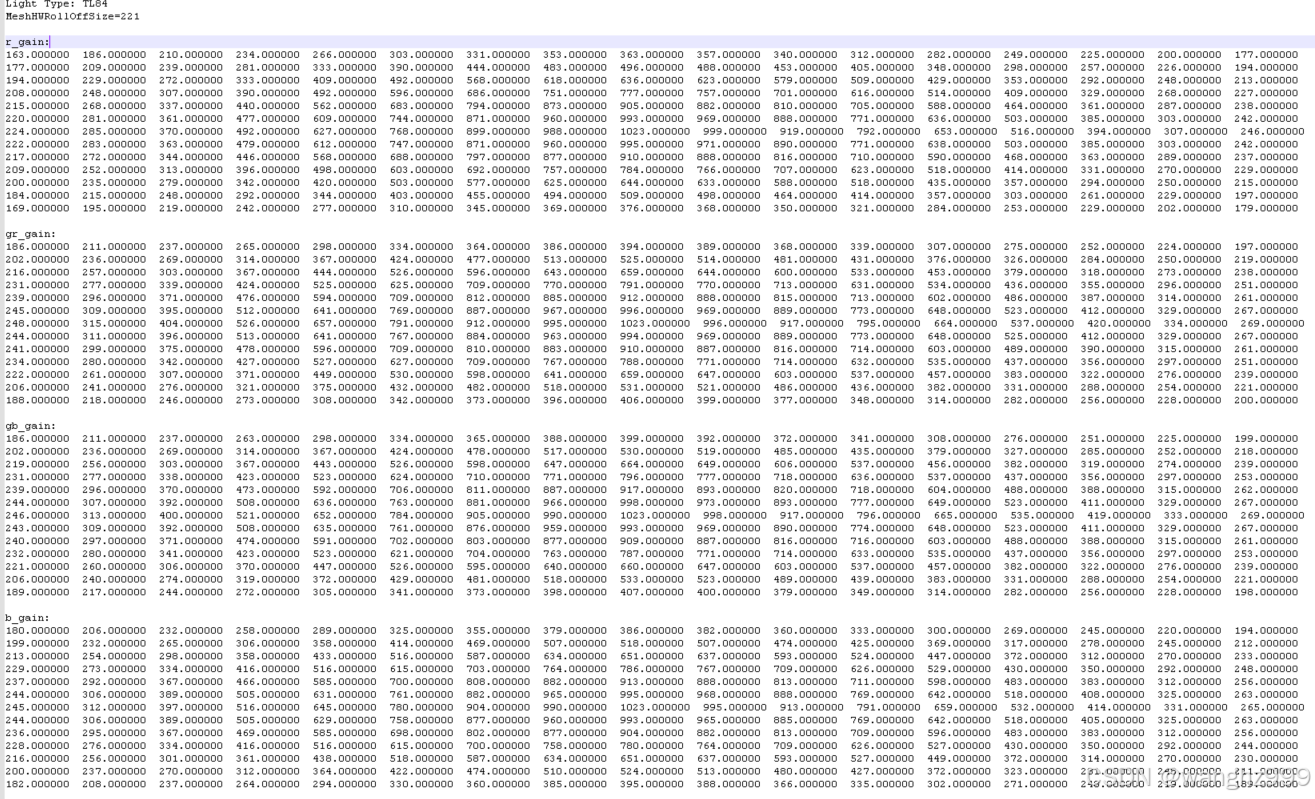
LSC OTP数据示例:
multicamera配置
高通Camera会根据
vendor/qcom/proprietary/chi-cdk/oem/qcom/multicamera/chimcxcameraconfig/configs中的配置与DTS中的配置对应然后找到具体加载哪一份配置
netrani/netrani_dc.xml
<Devices
  xmlns:xsi="http://www.w3.org/2001/XMLSchema-instance"
  xsi:noNamespaceSchemaLocation="../../../tools/logicalcameragenerator/logicalcam.xsd">
    <PhysicalDevice name="RearPhysicalCam"     slotId="6" cameraId="0" sensorName="ov13b10"/>
</Devices>
编译
vendor/qcom/proprietary/chi-cdk/oem/Android.mk中指定了编译so文件:
include $(CAMX_CHICDK_OEM_PATH)/qcom/sensor/ov13b10/build/android/Android.mk
vendor/qcom/proprietary/chi-cdk/configs/product.mk:
PRODUCT_PACKAGES += com.qti.sensor.ov13b10
PRODUCT_PACKAGES += com.qti.sensormodule.united_ov13b10.bin
PRODUCT_PACKAGES += com.qti.tuned.united_ov13b10.bin
vendor/qcom/proprietary/chi-cdk/oem/qcom/buildbins/build/android/binary_parrot会有相应的mk文件,指定了使用哪一个文件来生成:
qti.sensormodule.united_ov13b10.mk
##################################
# Generate camx binary file from XMLs

ifeq ($(CAMX_CHICDK_PATH),)
  LOCAL_PATH            := $(abspath $(call my-dir)/../../..)
  CAMX_CHICDK_PATH      := $(abspath $(LOCAL_PATH)/../../..)
else
  LOCAL_PATH            := $(CAMX_CHICDK_OEM_PATH)/qcom/buildbins
endif

include $(CLEAR_VARS)

# file name of the binary
CAMX_LOCAL_BIN := com.qti.sensormodule.united_ov13b10.bin

# the inputs to the binary
CAMX_LOCAL_BIN_INPUTS := sensor/ov13b10/ov13b10_sensor.xml      \
                        sensor/ov13b10/ov13b10_pdaf.xml        \
                        module/united_ov13b10_module.xml       \
                        eeprom/p24c64e_ov13b10_eeprom.xml           \
                        actuator/dw9714p_actuator.xml        \
                        flash/pmic_flash.xml

CAMX_BINARY_XSD_PATH  := $(CAMX_CHICDK_PATH)/api/sensor/

# The argument for the ParameterParser
# leave it blank if you are not sure about it.
CAMX_LOCAL_PARAMETERPARSER_ARG :=

# include the common settings for camx binary generation
include $(CAMX_BUILD_GENERIC_BINARY)